CE338 Digital VLSI Design Lab 2023 Fall
Lab 3 Layout of the R_2R DAC
Name: Jesse Moder
Email:
jmmoder@fortlewis.edu
1. Layout of the R_2R DAC
2. Introduction
Objectives:
a. Layout the R-2R DAC in Electric VLSI using N-Well resistors.
b. Be familiar with Electric VLSI and LTSpice for integrated circuit design.
3. Materials and Methods
Electric VLSI was used to layout an R_2R ladder schematic and subcell.
The layout of the n-well resistors was created and connected for the
10-bit ladder.
The 10 cells of the ladder and bottom resistor were created and
connected using the wiring tool. The DRC was checked heirarchically and
an NCC was ran on the schematic and layout views of the cell.
The R-2R ladder was connected to an imported ideal 10-bit ADC. The
circuit was exported to LTSpice for simulation with a sinusoidal input
of 5v.
4. Results
Figure 1 shows the R_2r ladder and the icon view created in Electric VLSI.
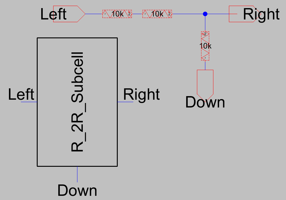
Figure 1: R_2R simplified circuit and subcell icon.
Figure 2 shows the subcells connected together to create version 2 of the R_2R ladder.
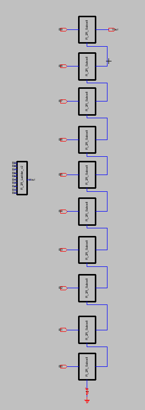
Figure 2: R_2R ladder and icon view.
Task 2
Figure 3 shows the layout of the subcell with the 10k n-well resistors and the connections of the 3 resistors per cell.
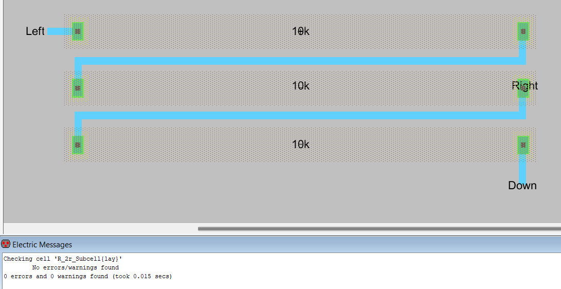
Figure 3: Subcell layout and confirmation of 0 errors.
Figure 4 shows a sample of the 10 layout cells placed and the error message window.
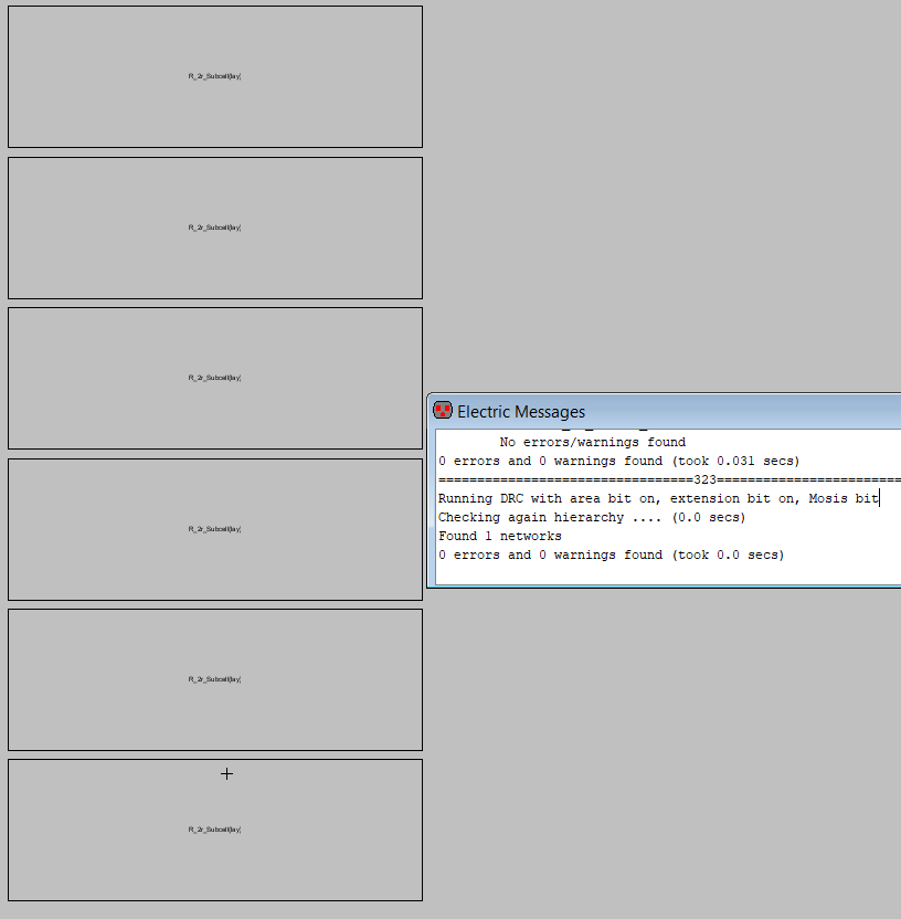
Figure 4: layout view of the R_2R ladder and error window.
Figure 5 shows the layout cells connected and the error message window with no errors.
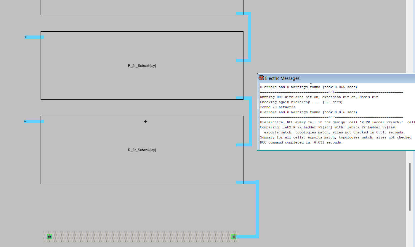
Figure 5: Sample of R_2R ladder layout connections and error window with no errors.
Figure 6 shows the 10_bit ideal ADC connected to the version 2 R_2R ladder with a siunusoidal input of 5V.
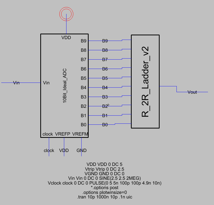
Figure 6: ADC connected to the R_2R ladder to be exported to LTSpice.
Figure 7 shows the simulation perfromed in LTSpice which was exported from Electric VLSI.
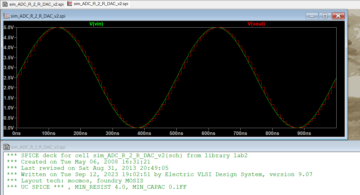
Figure 7: Spice simulation of the ADC connected to the R_2R ladder.
5. Discussion
This lab was very useful for learning subcell layout and component
placement. I had originally placed the layout subcells too close
together and the layout did not pass the MOSIS design rules.
I changed the spacing of the cells and the resistor and the design
passed. The input was sinusoidal with a peak of 5v, as expected. Vout
was stepped due to the analog output and matched the ideal ADC to DAC
output.
This lab highlighted the importance of following the design rules of
the manufacturer and being careful while laying out the schematic.