CE338 Digital VLSI Design Lab 2023 Fall
Lab 2
Design an R-2R DAC
Name: Jesse Moder
Email: jmmoder@fortlewis.edu

1.
Design an R-2R DAC
2. Introduction

Electric VLSI software is very useful for modeling and simulating circuits. The software is easy to learn and has a large database of components to model with. The software checks for errors in the design and helps locate the errors for troubleshooting. The models easily export to LTSpice for simulation. Modeling and simulating circuits are both important steps in circuit design and make the design process efficient and straight forward.

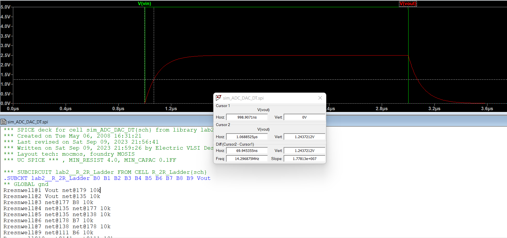
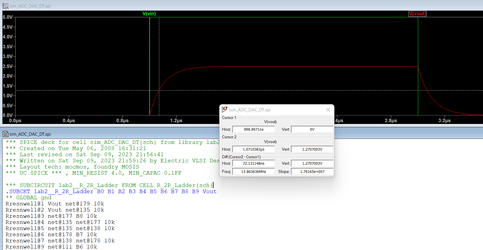
Calculated Rth for task 3: With B9 as the only input, B0-B8 were connected to ground and the circuit was reduced to the 20k resistor between B9 and Vout parallel with the equivalent resistance of the rest of the circuit. The rest of the circuit resistance simplified to 20k.

(1/20k+1/20k)^-1 = 10k

Calculated Vdd = 5V * 10k/20k = 2/5V

Calculated time delay for task 3: time delay = 0.7RC = 0.7*10*(10^3 ohm)*10*(10^-9 F) = 70 ns

3. Materials and Methods
Task 1:
The ENGR 338 Electric VLSI libraries were imported and the 10-bit ADC to DAC schematic was selected for simulation. The schematic was exported to LTSpice for simulation to confirm the libraries and file paths were correct.

Task 2:
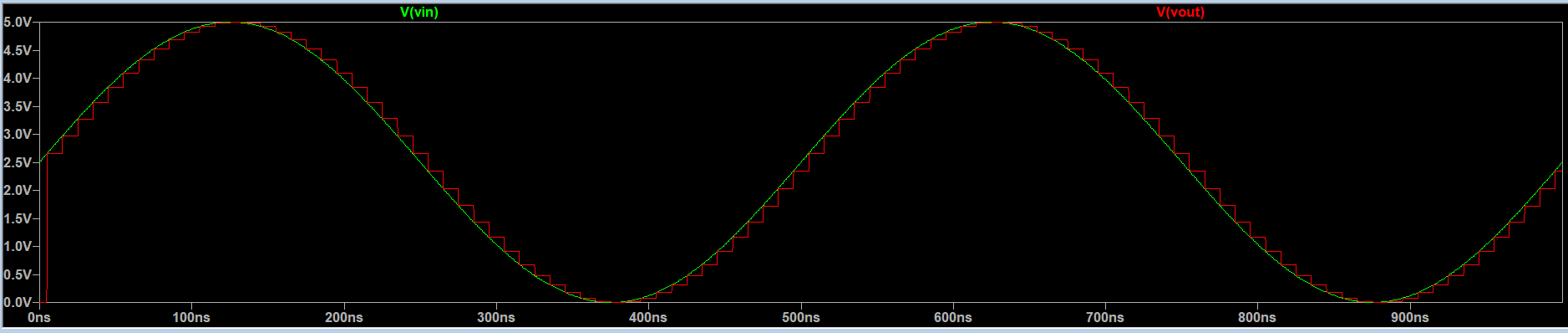
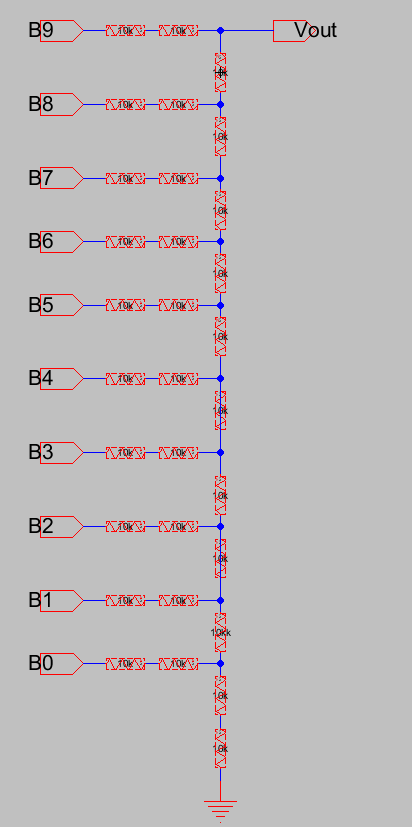
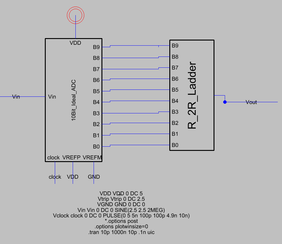
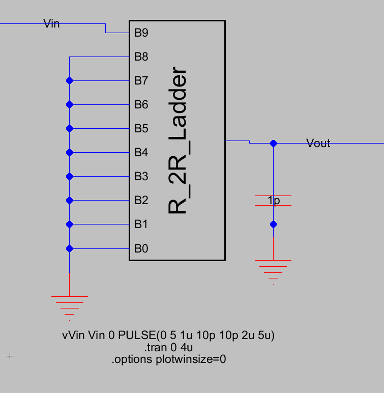
Electric VLSI was used to create a schematic of the R2_R ladder. An imported model of an analog to digital converter (ADC) was connected to the schematic of the R2_R ladder. The shematic was exported to LTSpice and was simulated with an input of 5V.

Task 3:
The R2_R ladder was simulated with an input to node B9 while the other nodes B0-B8 were connected to ground. A 10pF capacitor was connected to Vout. The input voltage was set to 5V. The time delay was measured using two cursers on the plot measuring the difference between 0V and 1/2 of the full scale voltage 1/2 Vdd, which is 1/4 Vdd or 1.25V. This value was compared to the theoretical value of 0.7RC, or 70ns.

4. Results (Your data/figure should have a caption. Figures should be labeled/numbered.)

Figure 1 shows the libraries were installed correctly and the ADC_DAQ loaded the correct scehmatic into Electric. Figure confirms the file path to load the spice deck was working and the voltage in and out were 5V, as expected.
ADC_DAQ
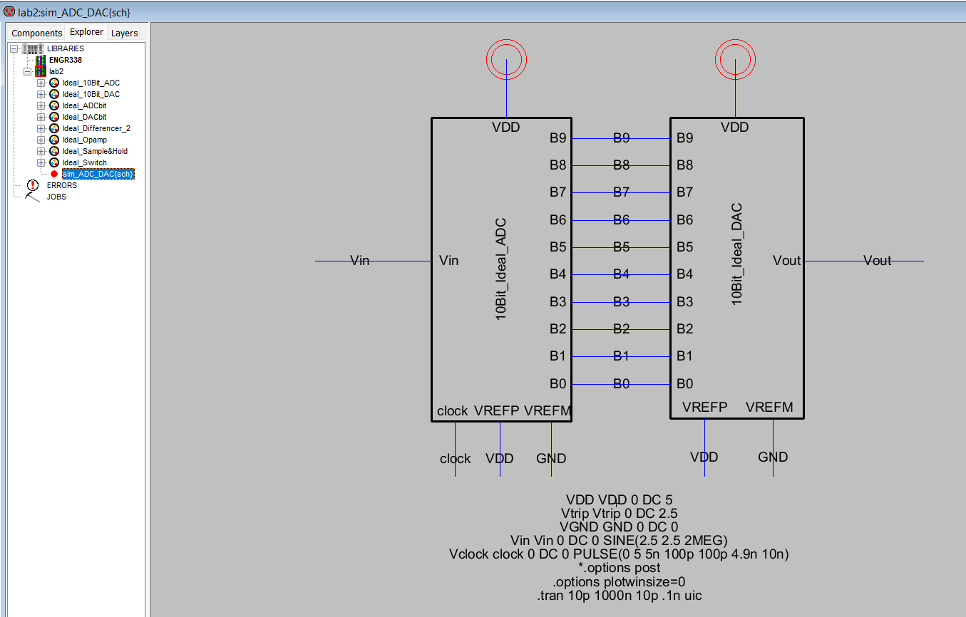
Figure 1: The shchematic of the ADC_DAQ loaded into Electric.

spice deck
Figure 2: The spice simulation of the ADC_DAQ peaked at 5V as expected and the output had a stepped pattern.

Figure 3 shows the R2_R ladder modeled using Electric, and Figure 4 shows the R2_R ladder and the icon view of the DAQ.
ladder
Figure 3: The R2_R DAQ schematic made using Electric.

ladder icon
Figure 4: The R2_R DAQ schematic and the icon view made using Electric.

Figure 5 shows the R2_R DAQ connected to the 10-bit ideal ADC imported from the library. Figure 6 shows the spice simulation of the voltage in and out with a 5V pulse input.
daq ladder
Figure 5: The ADC wired to the R_2R ladder and the spice code used for simulation.

ladder sim
Figure 6: The spice simulation of the ADC connected to the R2_R ladder. The simulation matches the ADC_DAQ simulation from the library provided.

Task 3:

Figure 7 shows the R_2R ladder with a 5V pulse input and a 10 pF capacitor connected to the output.
task 3 ladder
Figure 7: The Electric schematic for simulating the output of the R_2R ladder when B9 is the only input.

Figure 8 shows the time delay when the cursor was set to 1.24V, just under the 1.25V desired value.
R_2R ladder sim
Figure 8: The spice simulation for the input and outut voltages of the R_2R ladder and the measured time delay at 1.24V.

Figure 9 shows the time delay when the cursor was set to 1.27V, which was greater than the 1.25V desired value.
task 3 sim 2
Figure 9:
The spice simulation for the input and outut voltages of the R_2R ladder and the measured time delay at 1.27V.

5. Discussion

The libraries and file paths were installed correctly and the ideal 10-bit ADC_DAQ simulation was exported to LTSpice. The output was stepped as expected for an analog output from a DAQ.

The simulation for the R_2R ladder modeled for task 2 matched the ideal 10-bit ADC_DAQ voltage input and output.

For task 3, the time delay measured from the simulation plot appeared to match the 70 ns value from the theoretical calculation. The cursor did not align with exactly 1.25 V, but 1.24 V had a time delay of 69.9 ns and 1.27 V had a time delay of 72 ns.