CE338 Digital VLSI Design 2023 Fall
Course Project
Name: Jesse Moder
Email:
jmmoder@fortlewis.edu
1. Course Project Part 1
2. Introduction
A successive-approximation-register analog-to-digital converter (SAR ADC) is a low-power, low-footprint
ADC useful for small, portable devices. The SAR ADC works by comparing
the digital ouput to the input analog signal with successive
aprroximations until the final digital output is reached, and the
resolution is typically 8 or 16 bits.
3. Materials and Methods
ElectricVLSI was used to create a SAR ADC. A 3-bit NAND gate was first constructed and then used to
create a TI Set/Reset Data Flip Flop. The icon for the DFF was used to construct the sequencer and register with nine
DFFs for each component. The connections between the sequencer and register were made to construct
the SAR ADC. The icon for the SAR ADC was used to simulate the logic. The simulation was exported to LTSpice.
4. Results
Figure 1 shows the schematic of the 3-bit NAND gate using CMOS components.
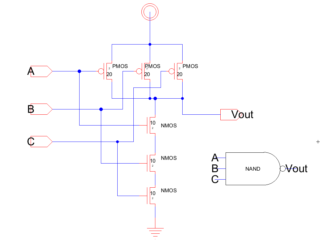
Figure 1: Schematic of the 3-bit NAND gate.
Figure 2 shows the schematic of the TI Set/Reset DFF constructed using 3-bit NAND gates, the icon view, and the DRC.
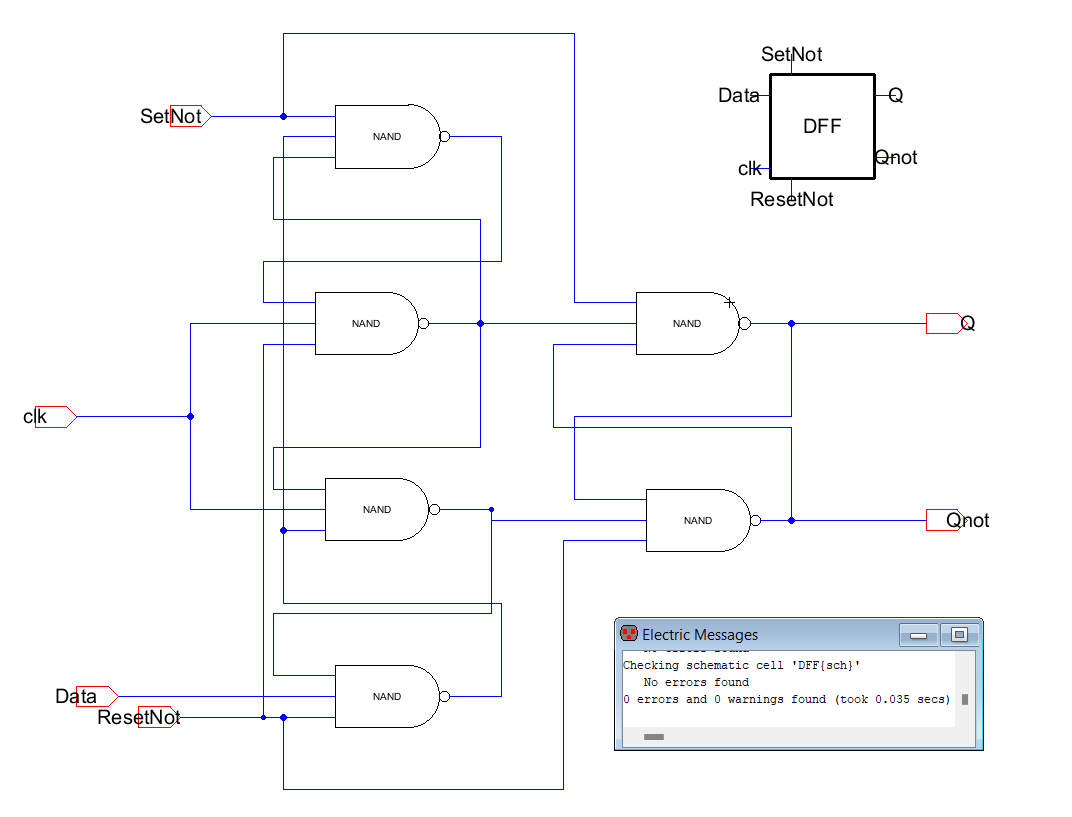
Figure 2: TI Set/Reset DFF schematic.
Figure 3 shows the schematic of the SAR ADC constructed using the DFF icons, the icon view of the SAR ADC, and the DRC.
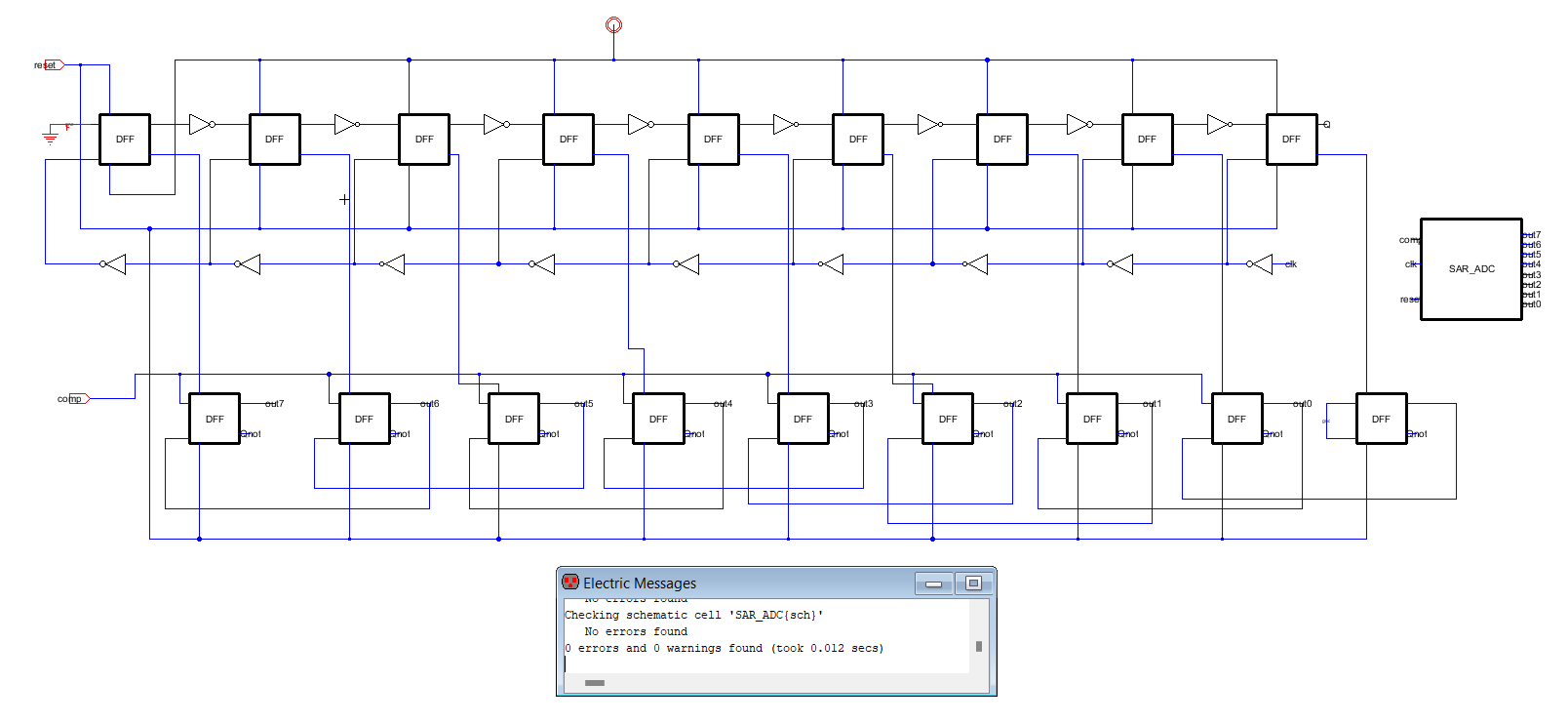
Figure 3: SAR ADC schematic.
Figure 4 shows the simulation schematic inputs and outpus of the SAR ADC and the DRC.
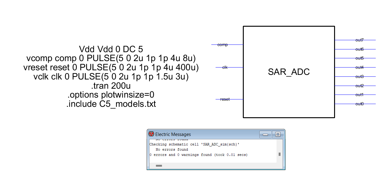
Figure 4: SAR ADC simulation schematic.
Figure 5 shows the LTSpice simulation results from the SAR ADC.
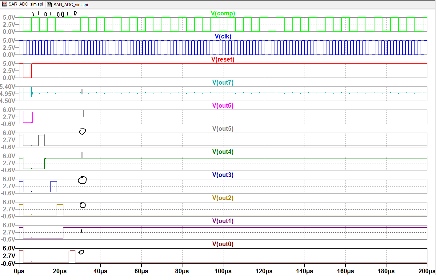
Figure 5: LTSpice simulation results of the SAR ADC.
5. Discussion
Creating the SAR ADC in ElectricVLCI was challenging because I had
created the schematics using some techniques that work for LTSpice. I
had created exports to vdd and ground in the 3-bit NAND schematic so I
shorted all of the Vhigh and Vlow connections together on the DFF and
SAR ADC schematics. The schematics had DRC errors since I used the
global symbols for vdd and ground as well as using exports. Once I
removed the exports and only used the global symbols for vdd and
ground, I no longer had to connect the Vhigh in the schematics, except
for the reset_not of the first DFF and the set_not of the following
eight DFFs. The DRC erros resolved and the DFF and SAR ADC worked as
expected. Creating the SAR ADC was good practice for the future tasks
of the course project.