Lab 9 Design an ALU
Jesse Duran
Spring 2021
ENGR 338
Introduction:
In this lab we create an ALU using our full adder developed previously.
The schematic and layout will be made. Our ALU will be able to do AND, OR, ADDITION, and SUBTRACTION.
Results:
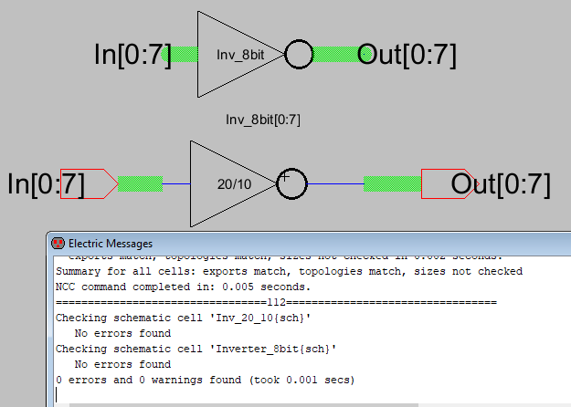
Figure 1. 8-bit inverter DRC clean
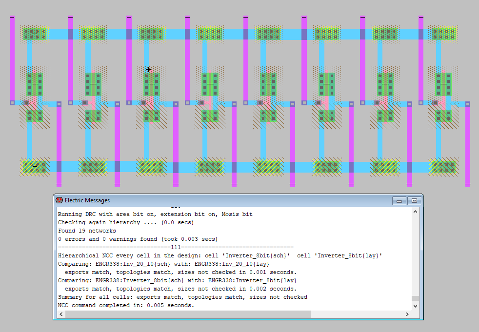
Figure 2. 8-bit inverter Layout DRC and NCC clean
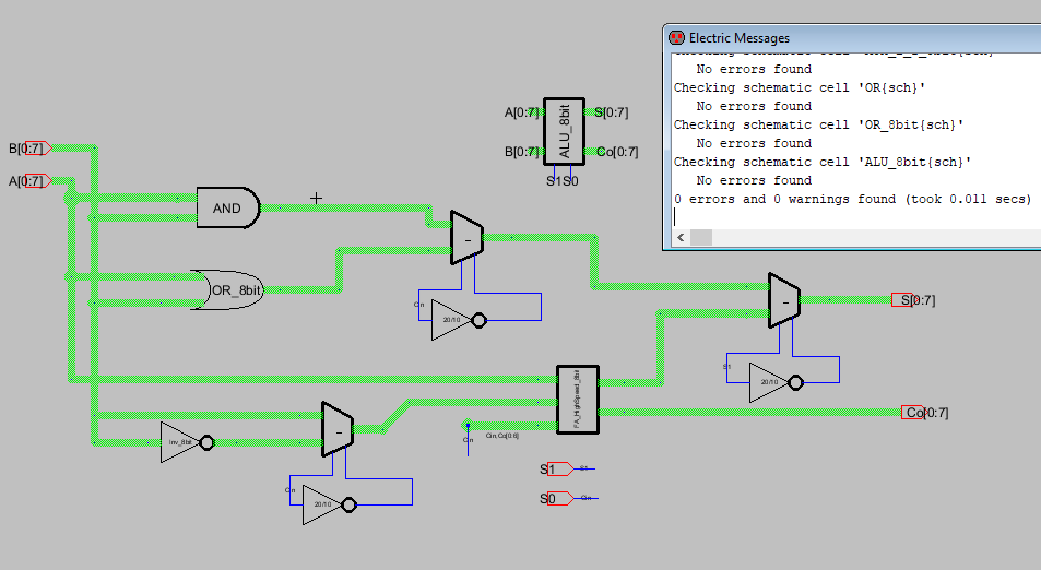
Figure3. 8-bit ALU schematic and layout DRC clean
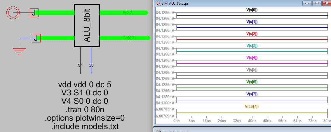
Figure 4. 8 bit ALU AND simulation. Working as expcted, outputs all 0s
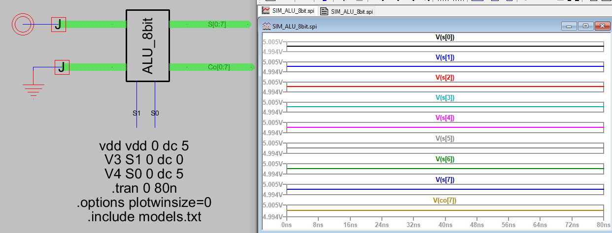
Figure 5. 8 bit ALU OR Simulation. Working as expected, all outputs 5V
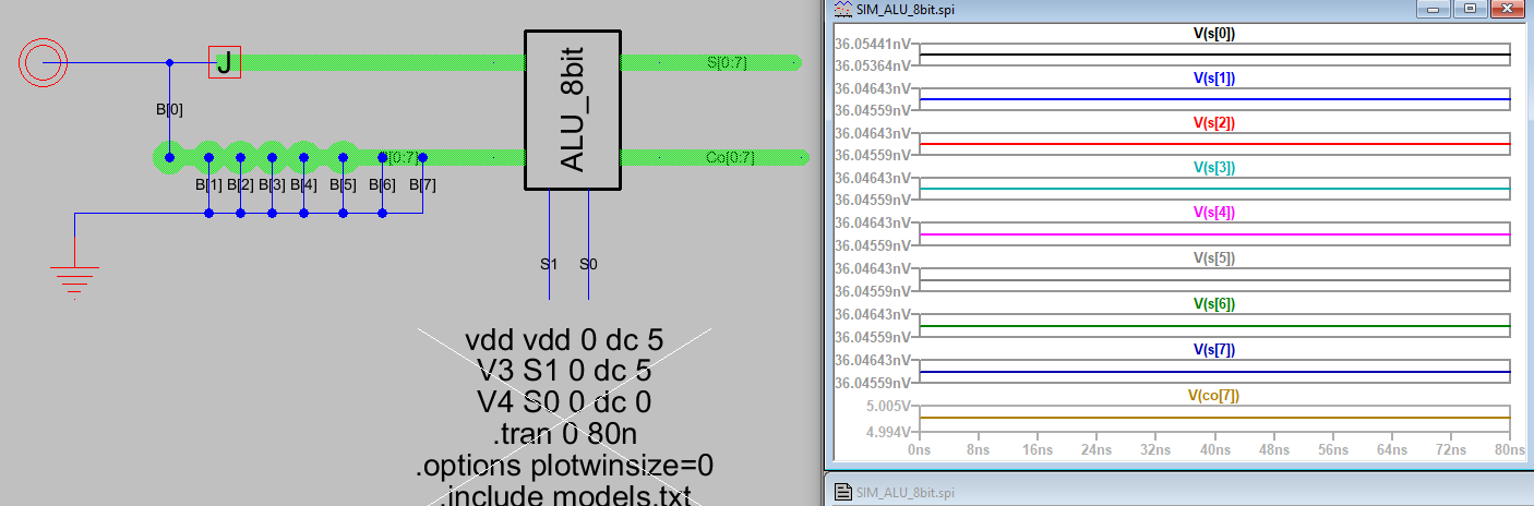
Figure 5. 8 bit ALU ADD Simulation. Working as expected, Output =
00000000, CO =1
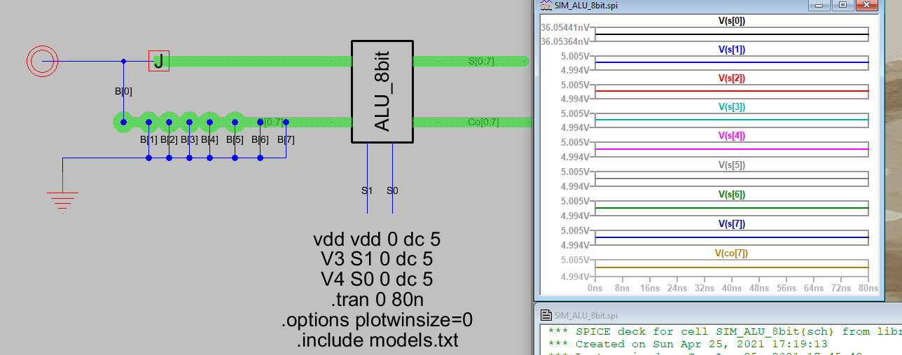
Figure 7. 8 bit ALU SUB Simulation. Working as expected, Output =
11111110, CO =1
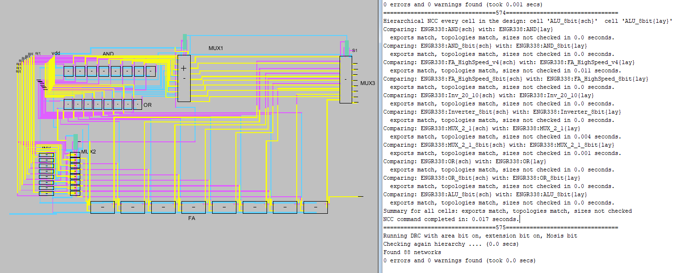
Figure 8. 8-bit ALU layout. DRC and NCC clean
Discussion
This lab was the most invloved one yet. It was the culmination of the
semester's work of building components. It was fun to see how each part
was used and why the 8-bit versions were being used. For the layout
portion, it was on us to figure out what connected where, it made us
understand the innerconnectivity and was a practice in planning