Lab 8 Design a MUX, and a High-Speed Full Adder
Jesse Duran
Spring 2021
ENGR 338
Introduction:
The goal of this lab was to create a 2-1 MUX and a High-Speed Full
adder. The mux was expanded to an 8-bit mux,. The High-Speed full adder
is faster than a traditional FA due to the smaller layout size which
decreased the operational time delay.
Task 1

Figure 1. 2 to 1 Mux schematic and icon DRC clean.
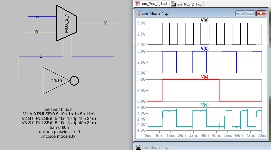
Figure 2. 2 to 1 MUX simulation. Logic verified.
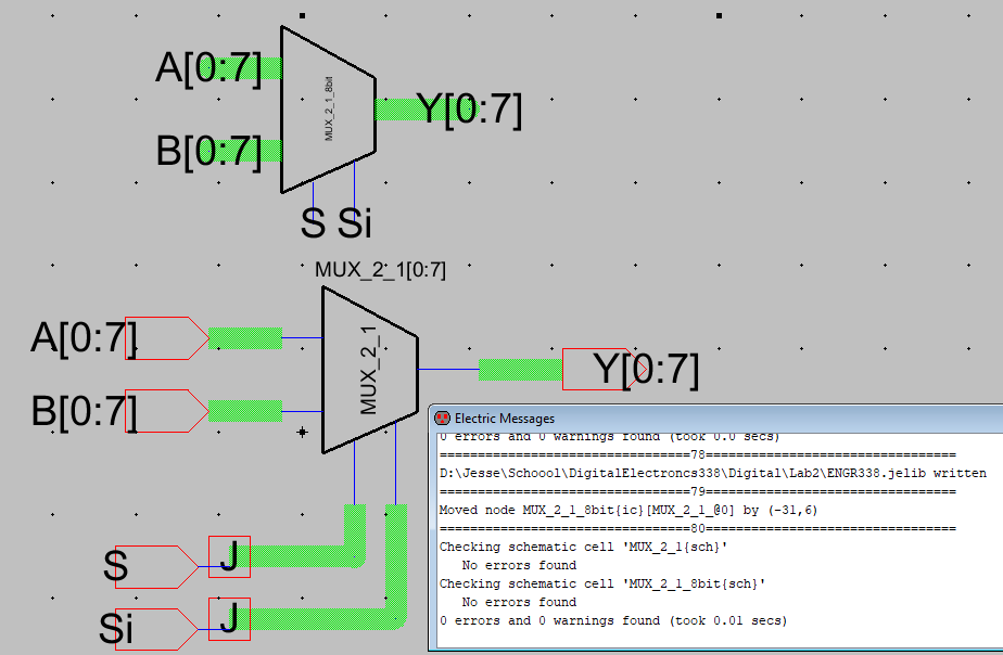
Figure 3. MUX_2_1_8bit schematic and icon DRC clean
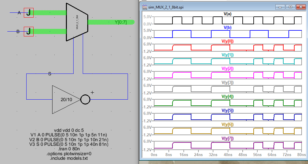
Figure 4. Simulation of 8 bit 2to1 Mux.
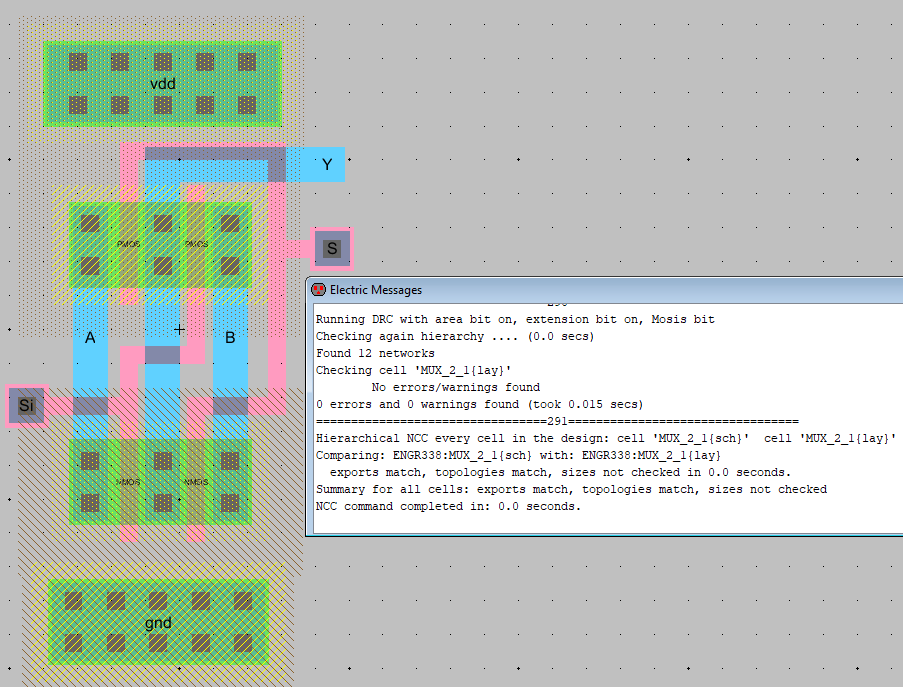
Figure 5. Layout of MUX_2_1 DRC and NCC clean
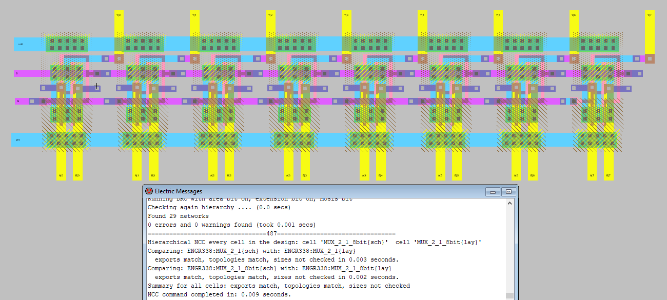
Figure 6. Layout of 8bit 2-1 MUX DRC and NCC clean.
Task 2:
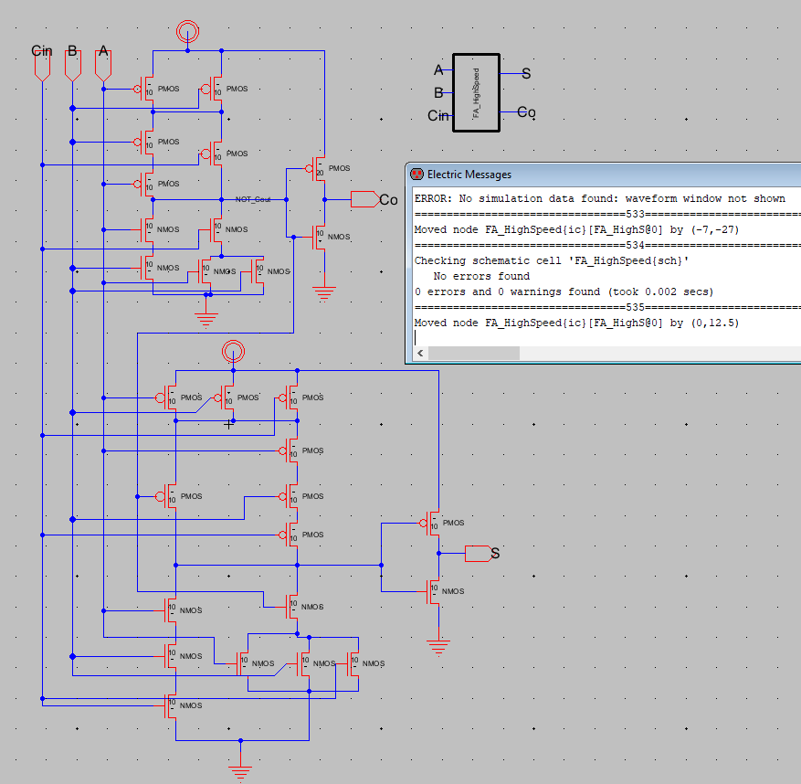
Figure 7. Full Adder High Speed schematic and icon. DRC clean
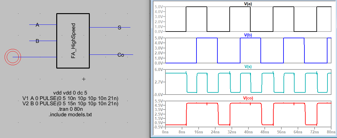
Figure 8. HighSpeed Full Adder simulation.
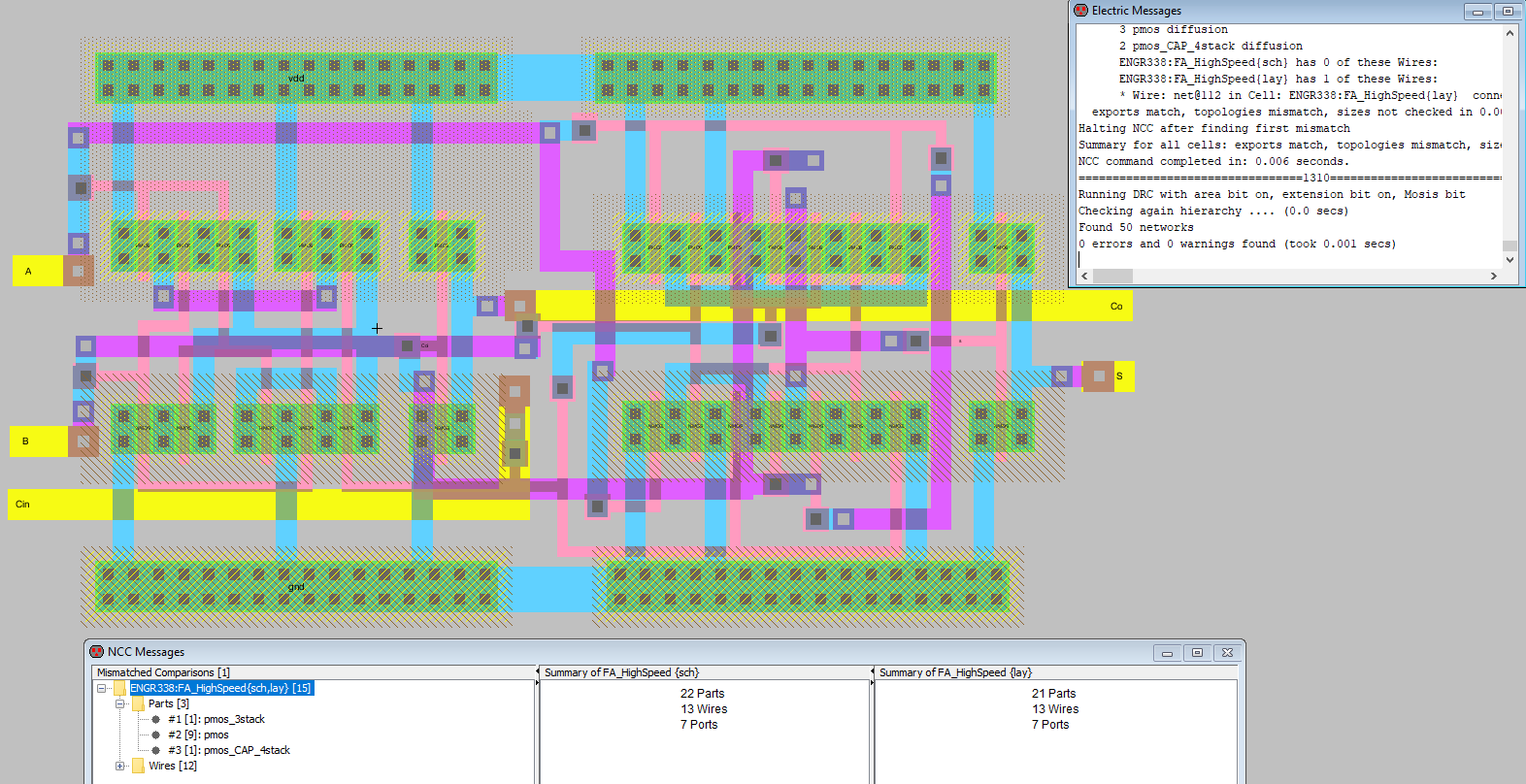
Figure 9. HighSpeed Full adder. DRC clean, NCC failed, one part is
missing in the first and second versions. I was unable to find the
errors
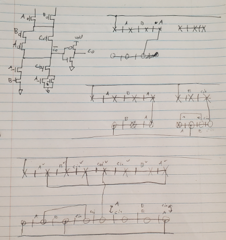
Figure 10. Stick diagrams of CO and S circuits.
Task 3
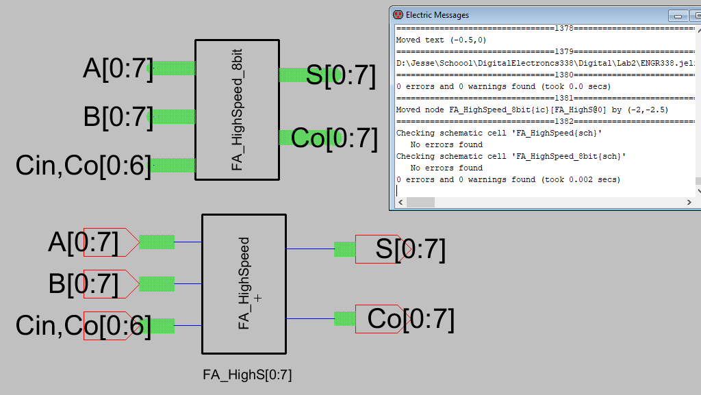
Figure 11. 8-bit highspeed full adder schematic and icon DRC clean
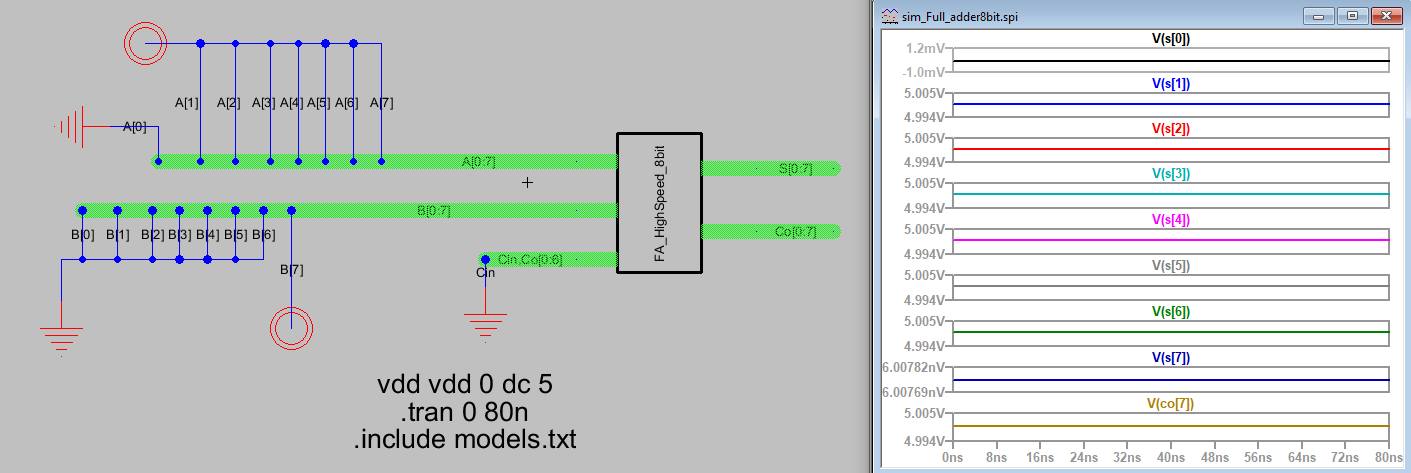
Figure 12. 8-bit Highspeed adder simulation. A="11111110", B="10000000", S ="01111110", Co=1
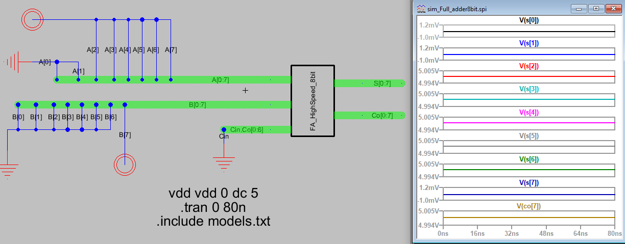
Figure 13. 8-bit Highspeed adder simulation. A="11111100", B="10000000", S ="01111100", Co=1
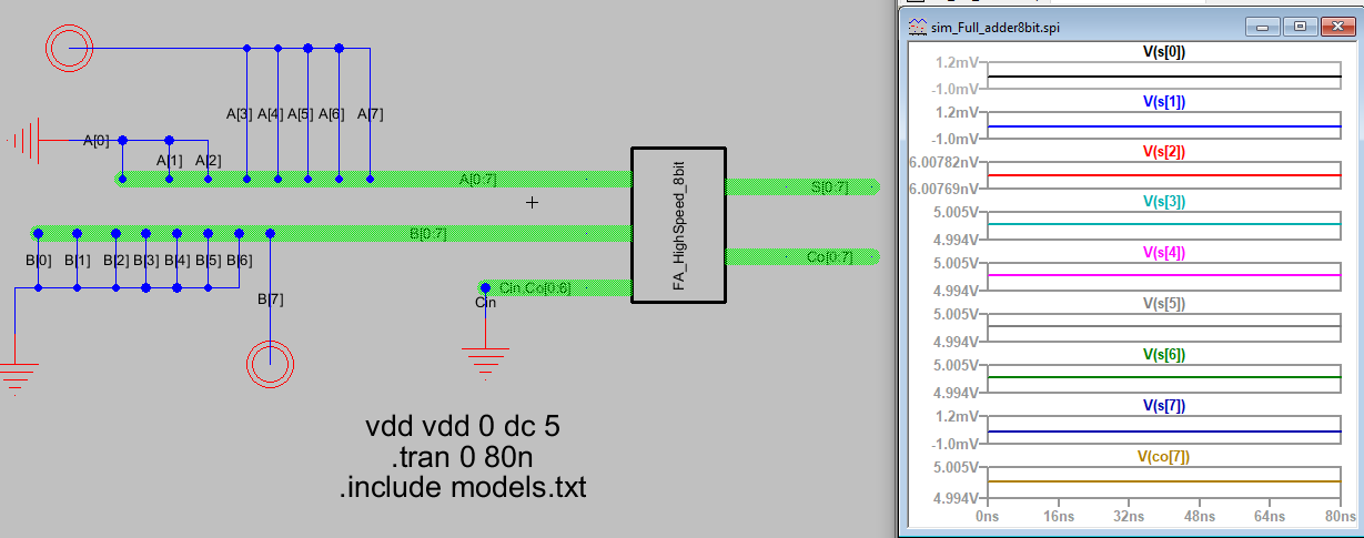
Figure 14. 8-bit Highspeed adder simulation. A="11111000", B="10000000", S ="01111000", Co=1
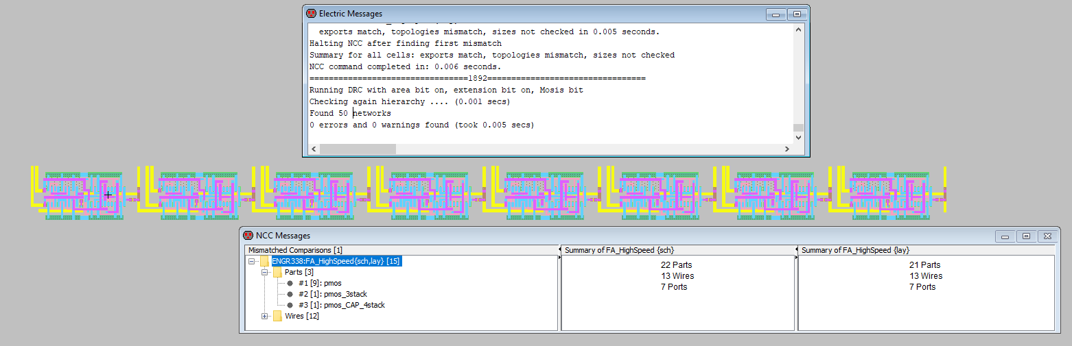
Figure 15. Layout view of 8bit high speed full adder. DRC clean, NCC failed with same issues as for the HS_FA layout.
Discussion
This lab reenforced making mulit bit components
from single bit component. We also learned how simplifying a circuit
can lead to a smaller layout and therefor a quicker operation time. I
faced issues with the layout for the highspeed full adder which may be
due to the splitting of PMOSs compared to the schematic. The array
function once again proved handy in making the larger bit components