Lab 6 Build a Nand, NOR, XOR, and Full Adder
Jesse Duran
Spring 2021
ENGR 338
Introduction:
The goal of this lab is to implement the logic gates, NAND, NOR, and
XOR, which will be used to build a full adder. This will require the
skills we have been developing over the previous labs to build a
fundimental digital component.
Task 1: Create the schematic and layout of the NAND gate
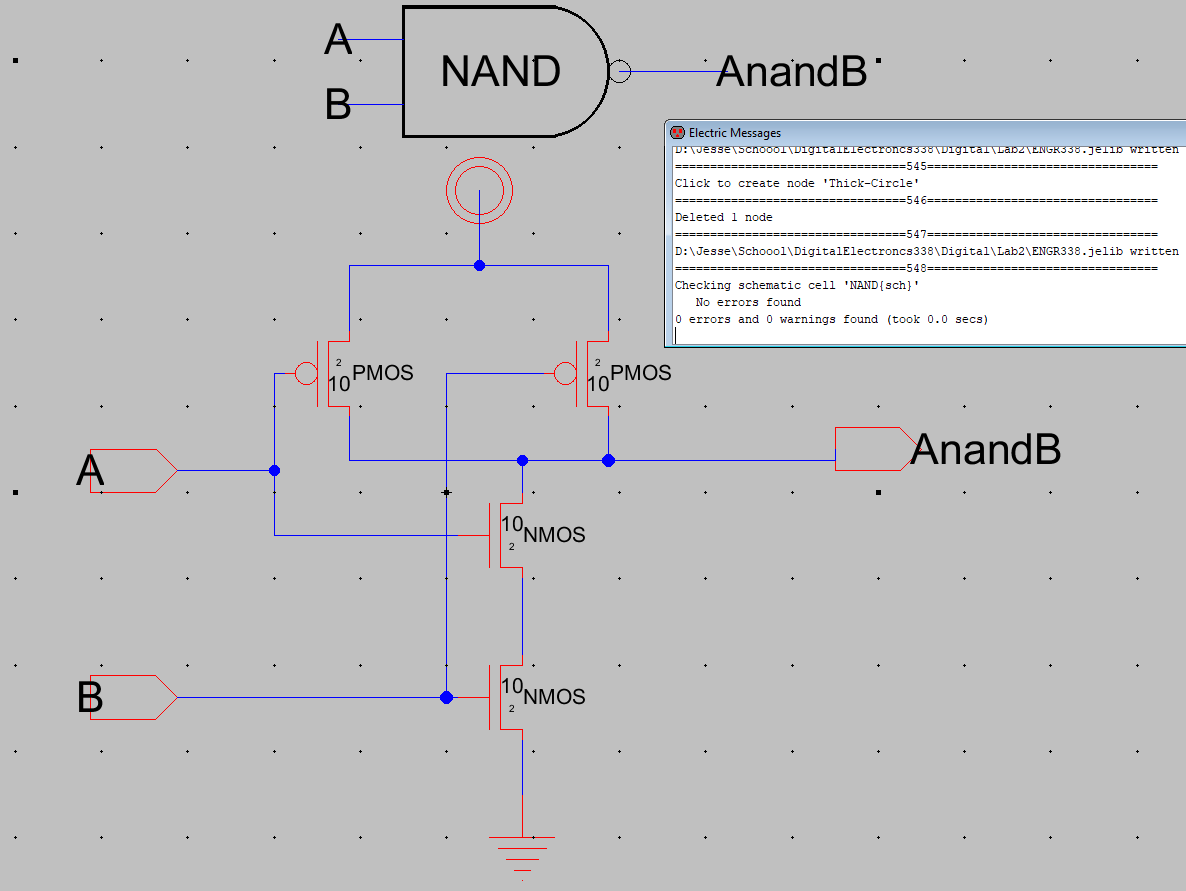
Figure 1. NAND gate Schematic, DRC clean.
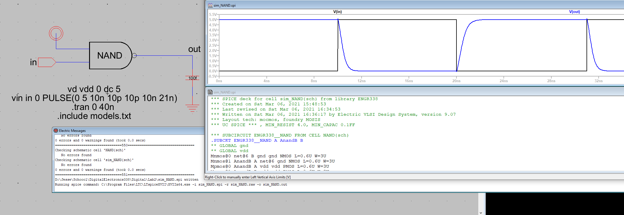
Figure 2. NAND simulaition using LTSpice.
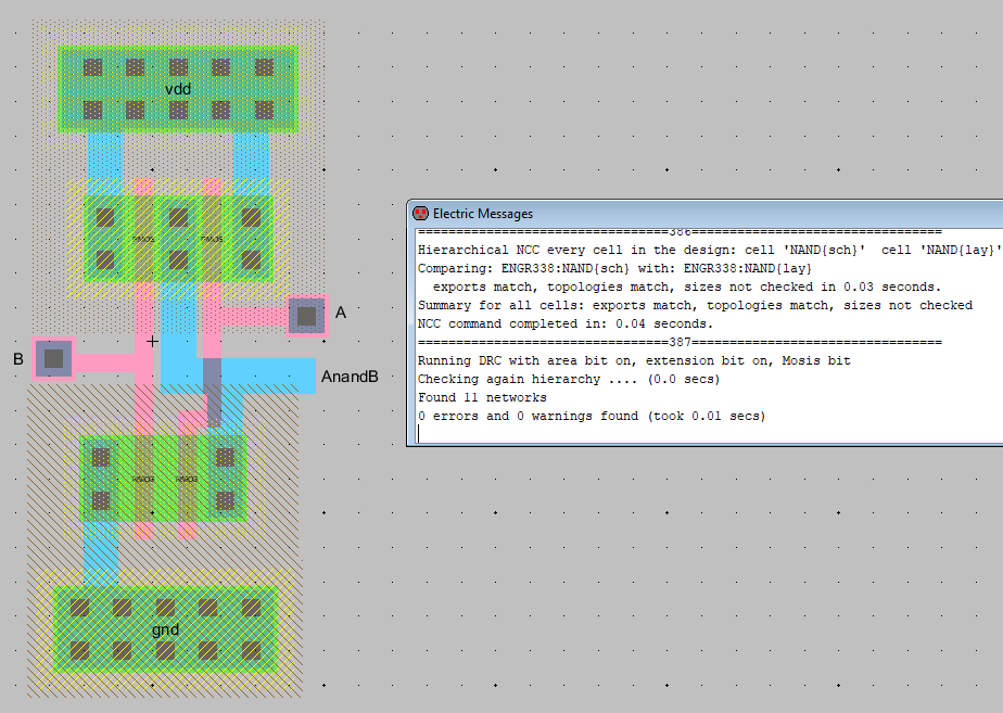
Figure 3. NAND layout constructed. DRC and NCC clean
Task 2: Creating schematic and layout for NOR gate
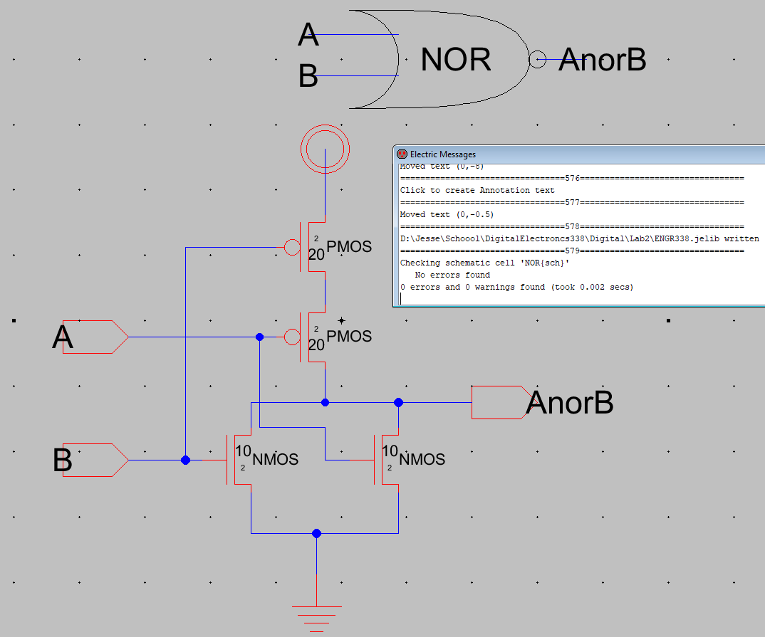
Figure 4. NOR schematic and Icon, DRC clean.
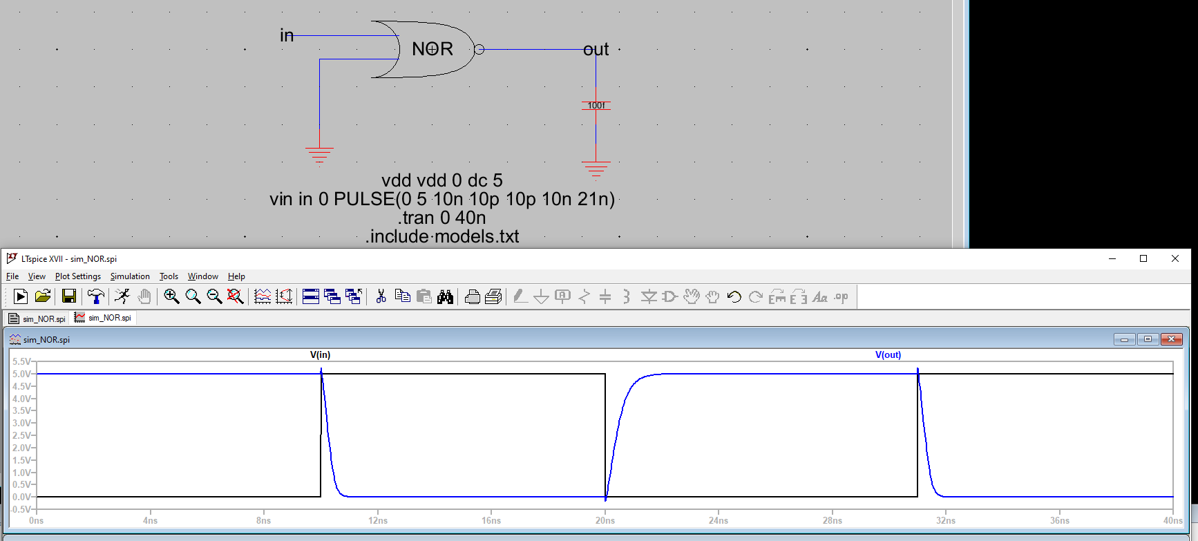
Figure 5. Simulation of NOR gate
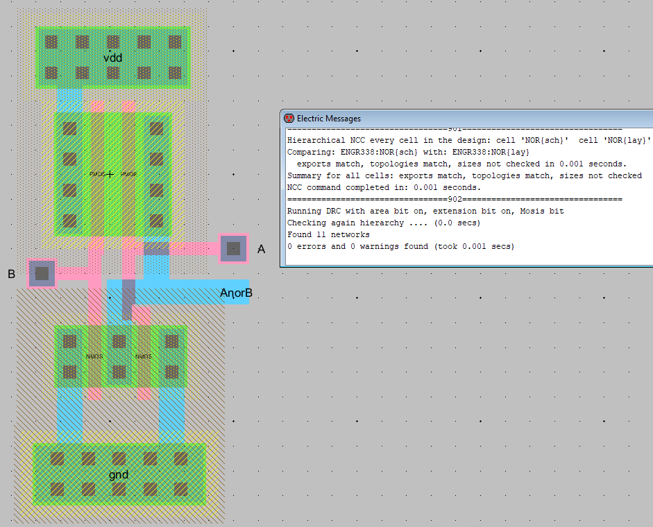
Figure 6. Layout of NOR gate. NCC match and DRC clean.
Task 3: Design, simulate, and layout an XOR gate
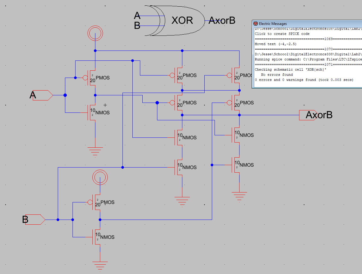
Figure 7. Schematic of XOR gate and icon. DRC clean
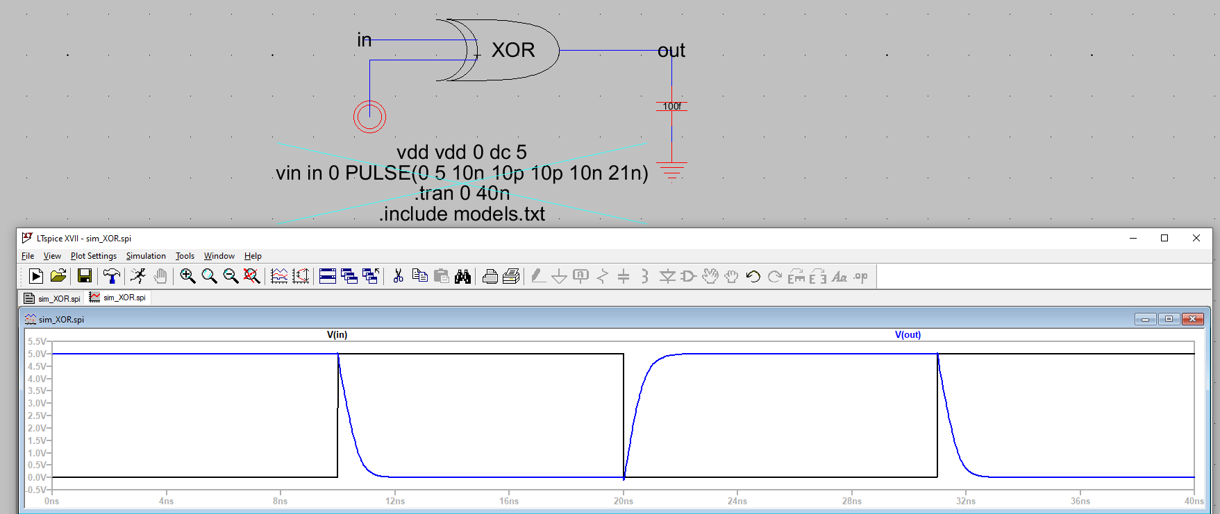
Figure 8. Simulation of XOR gate with B connected to VDD.
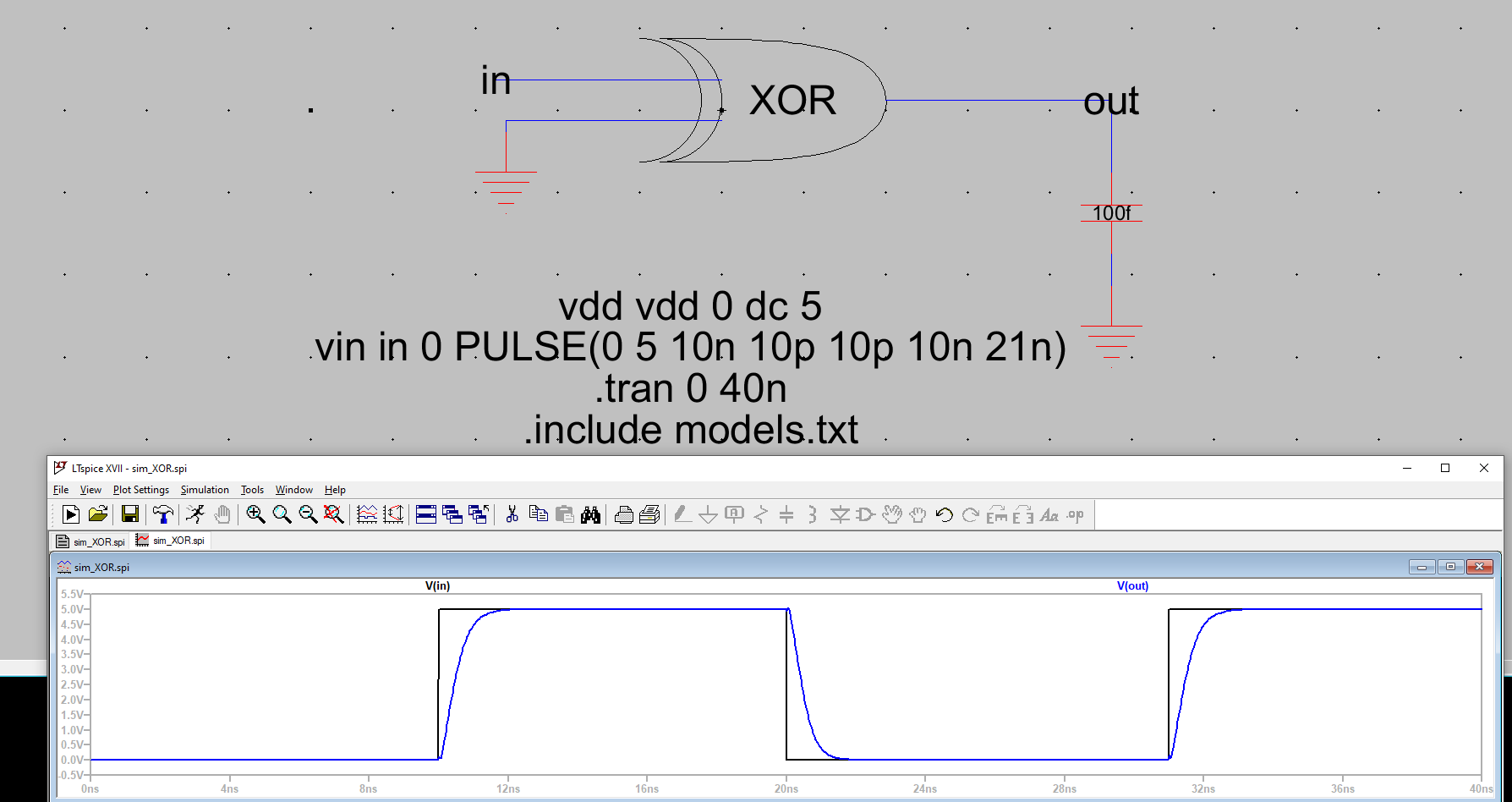
Figure 9. Simulation of XOR gate with B connected to ground.
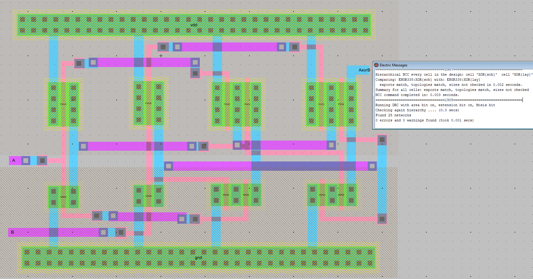
Figure 10. Layout of XOR gate, NCC matches and DRC clean.
Task 4: Full Adder
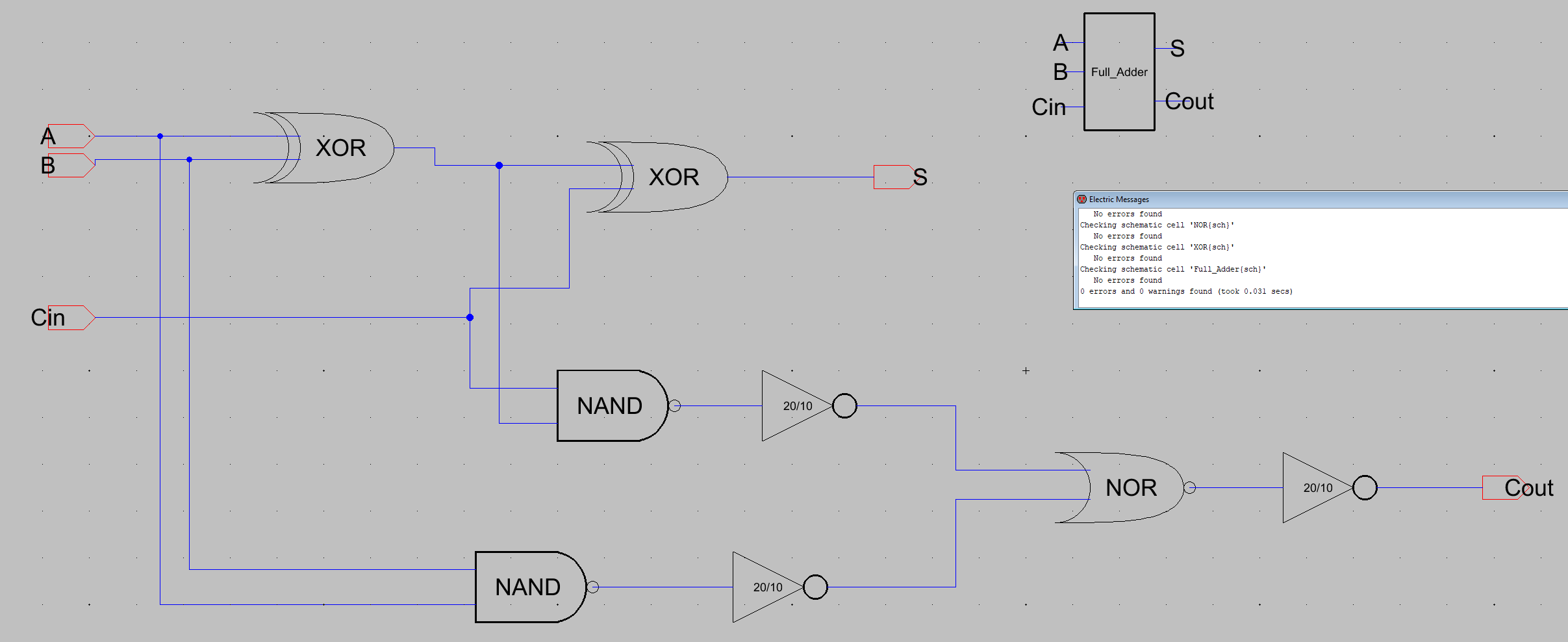
Figure 11. Full adder Schematic and icon. DRC clean.
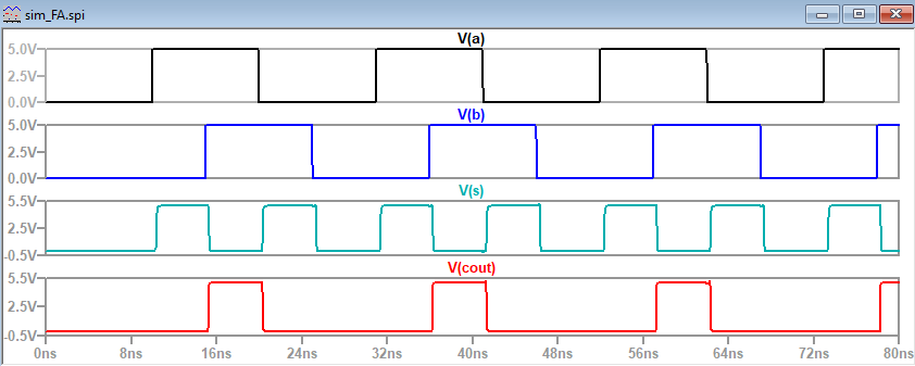
Figure 12. Full adder simulation with Cin grounded.
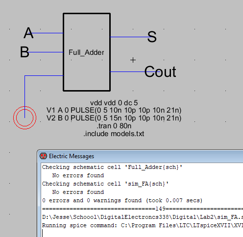
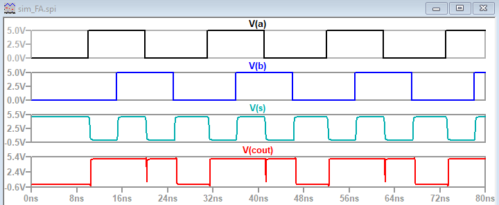
Figure 13. Full adder simulation with Cin connected to VDD.
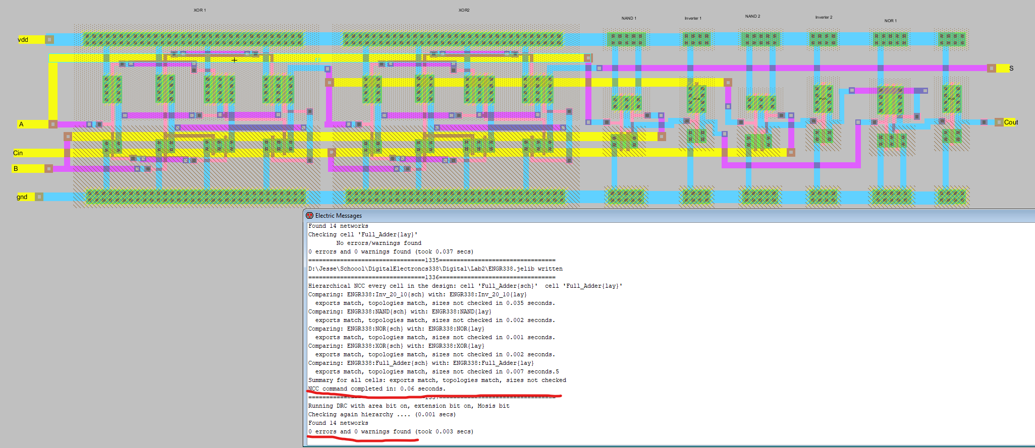
Figure 14. Layout of Full Adder using XOR, NAND, NOR, and INVERTER components. NCC and DRC clean
Discussion
Over the course of this lab we designed a full adder and all of the
gates needed to construct it. The reuse of gates is a good exersice in
resusiblity and the power of working from the ground up. The final
layout shows the need for understanding the differnt metal layers and
how to use them to prevent shorts. With the lessons in stick diagrams
it is evident how to use them to design a complex circuit such as the
full adder.