Students were tasked with laying out and creating schematics for NMOS and PMOS transistors using ElectricVLSI and C5 technology. The IV curves were then simulated using LTSpice. This teaches us about proper well connections to minimize body effect in our transistors.
3. Materials and Methods
ElectricVLSI was the used to layout the transistors and schematics. LTSpice was used for simulation of the IV curves; NMOS and PMOS specificaition were included in the C5_models.txt file. The tutorial followed can be found at Yilectronics.com
4. Results
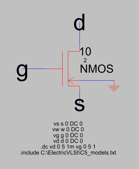
Figure 1. NMOS schematic and Spice code for simulation
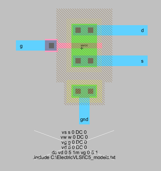
Figure 2. NMOS layout and Spice code for simulation
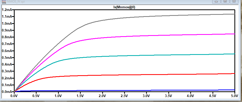
Figure 3. LTSpice simulation of NMOS I vs Vd curve from layout
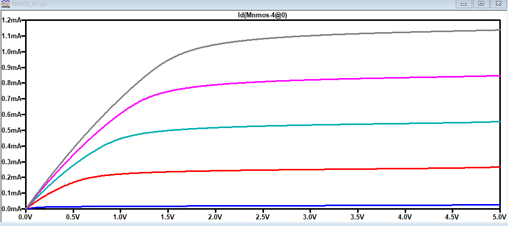
Figure 4. LTSpice simulaiton of NMOS I vs Vd curve from schematic
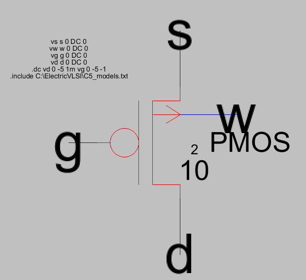
Figure 5. Schematic of PMOS with Spice code
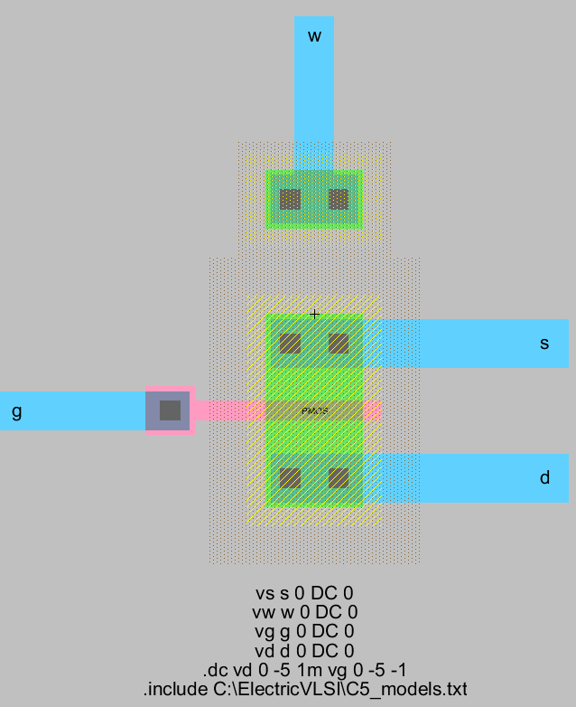
Figure 6. Layout of PMOS with spice code.
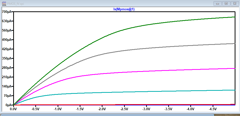
Figure 7. LTSpice simulation of I vs Vg from layout of PMOS
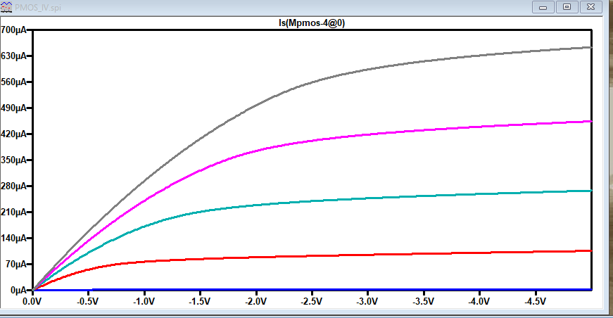
Figure 8. LTSpice simulation of I vs Vg from schematic of PMOS
5. Discussion
The concepts of how NMOS and PMOS are constructed from different doping concentraitions of silicone was reenforced by laying out the transistors. The power of simulation was shown again by being able to test our componants using LTSpice. The way that the transistors reach the onstate was demonstrated by the IV curves. We can visualize the pinch-off, linear, and cut-off regions in the IV curves