Lab 2 R-2R DAC
Jesse Duran
Spring 2021
ENGR 338
Introduction:
Over the duration of this lab we were
refamiliarized with ElectricVLSI and verified the function of a R-2R
Digital to Analog Converter.
Task 1
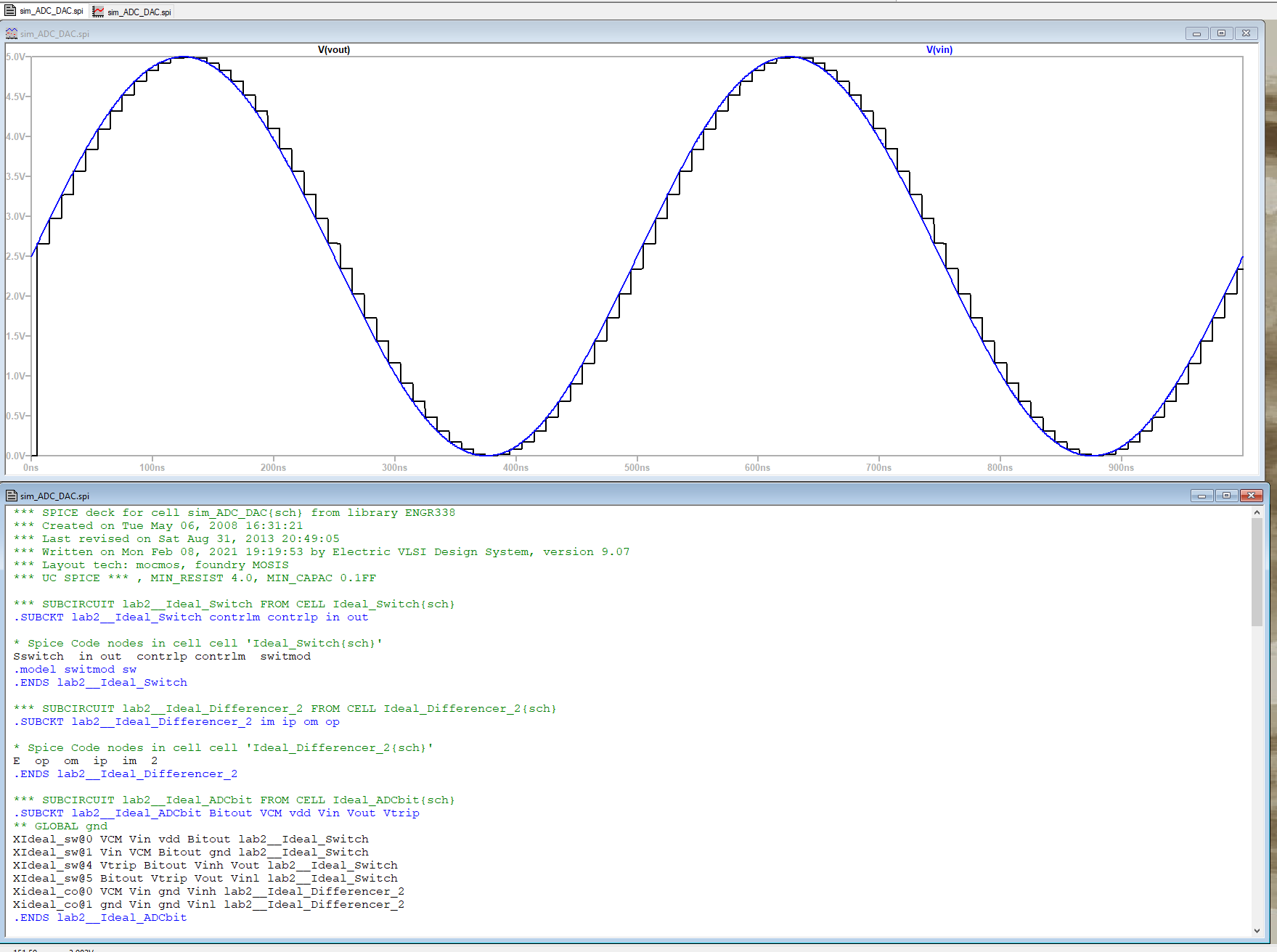
Figure 1. Vin and Vout from supplied Lab2.jelib library.
Task 2
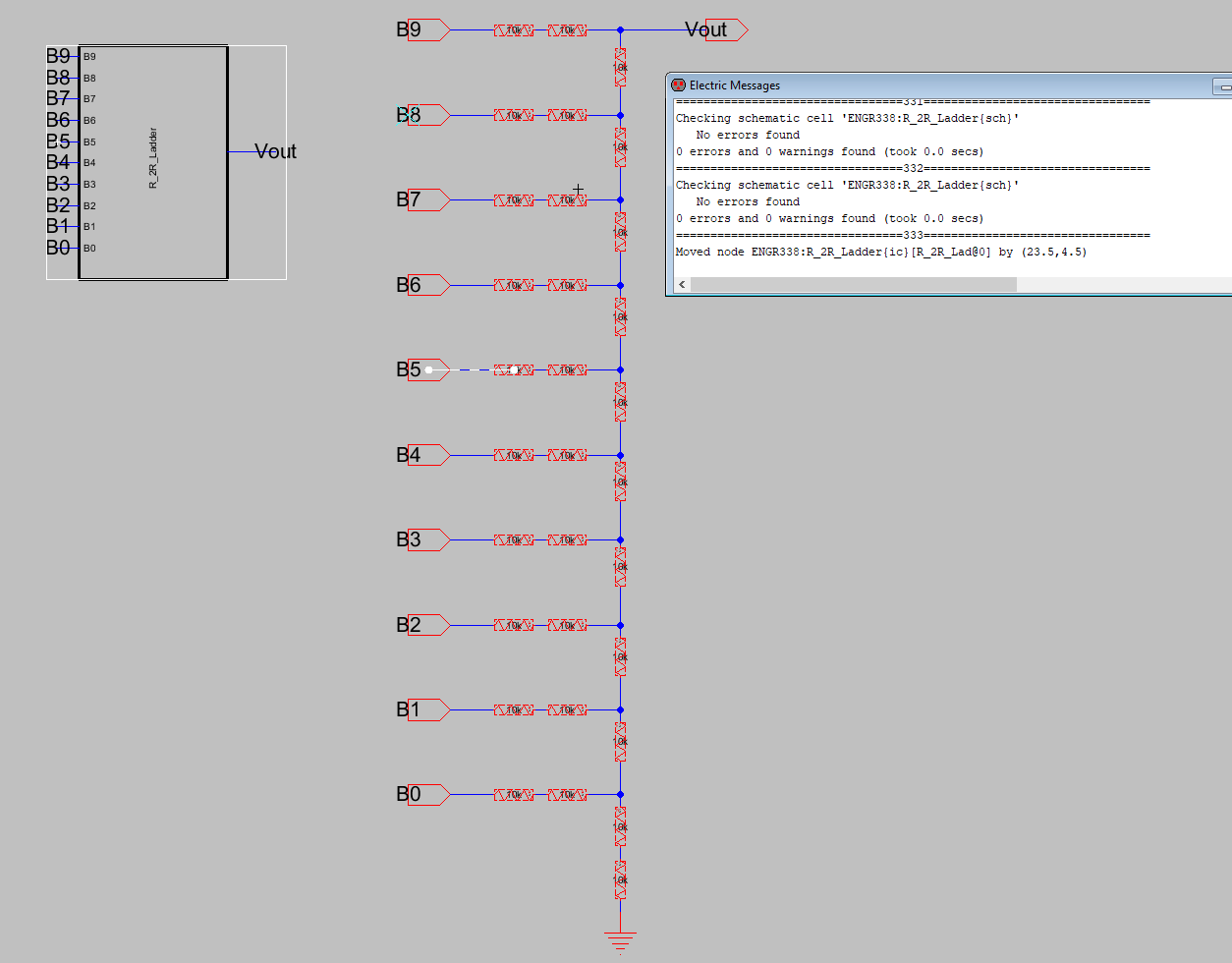
Figure 2. DRC Clean R-2R ladder. Icon visible
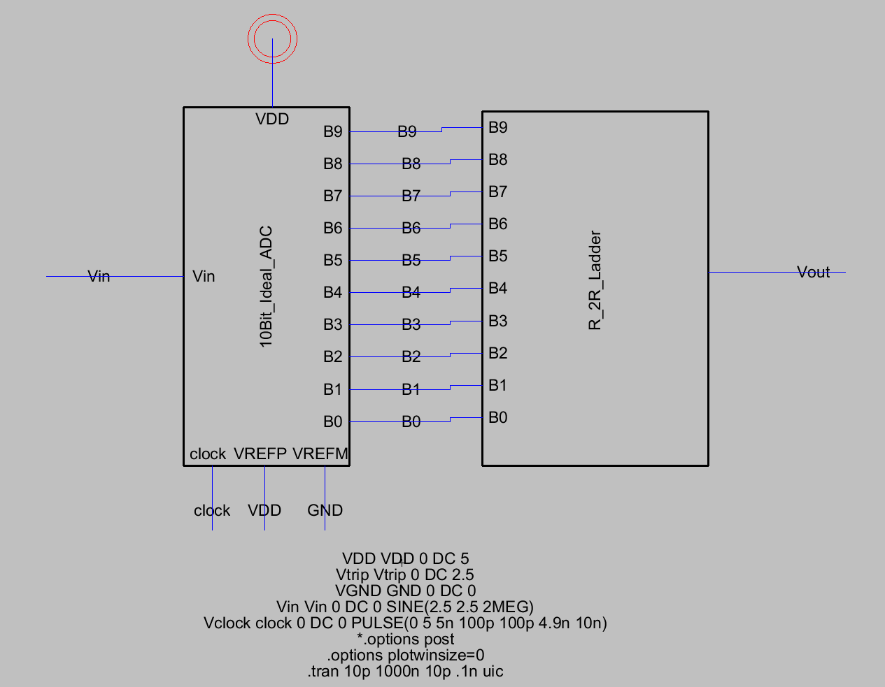
Figure 3. Simulation schematic for R-2R Ladder
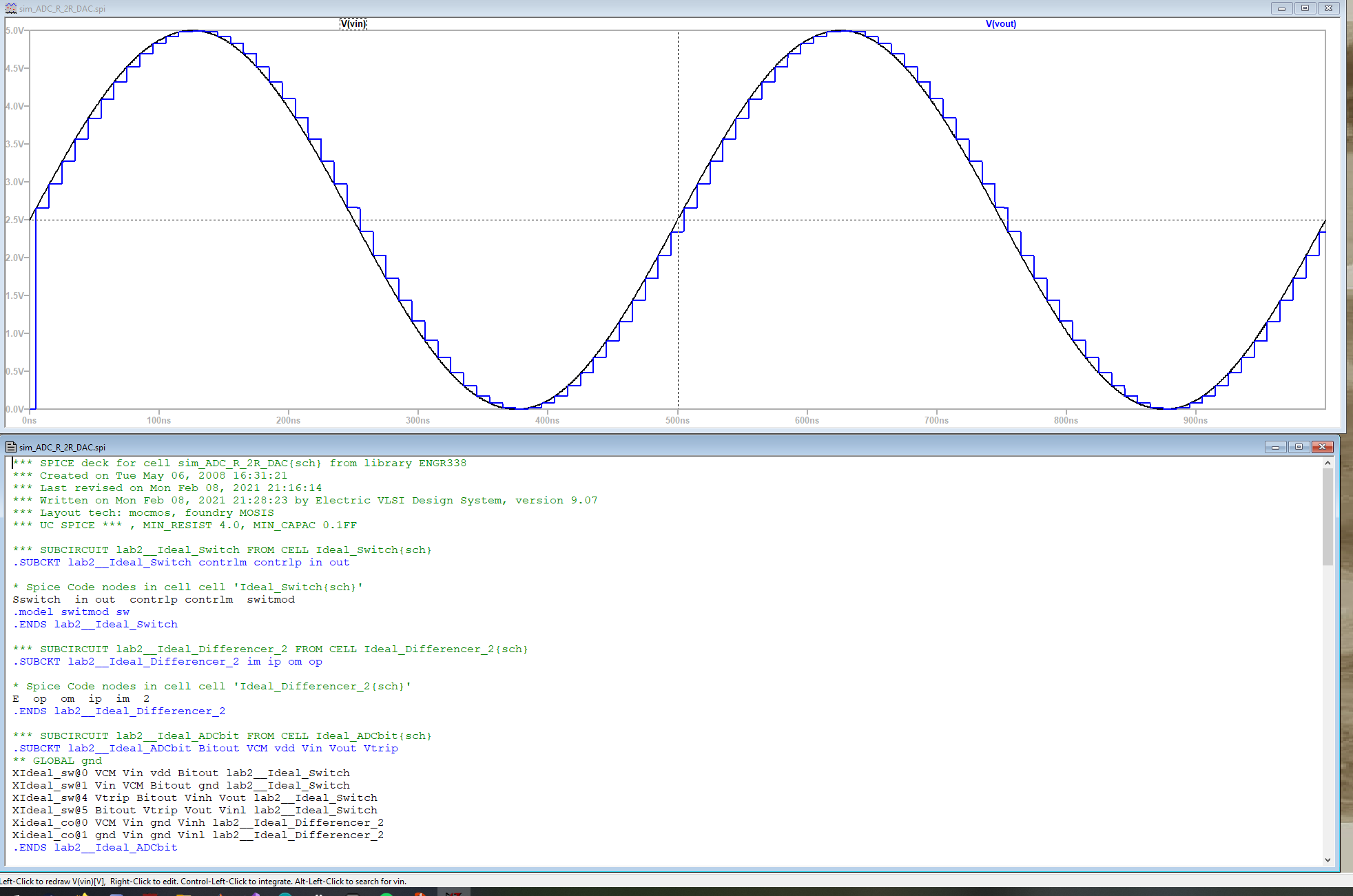
Figure 4. Simulation of R-2R Ladder DAC. Vin and Vout
Task 3
Calulation
TD = .7RC = .7(10k)(10p) = 70ns
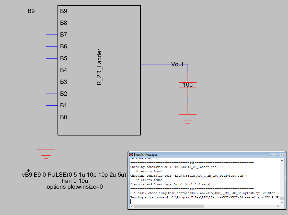
Figure 5. Time Delay simulation schematic.
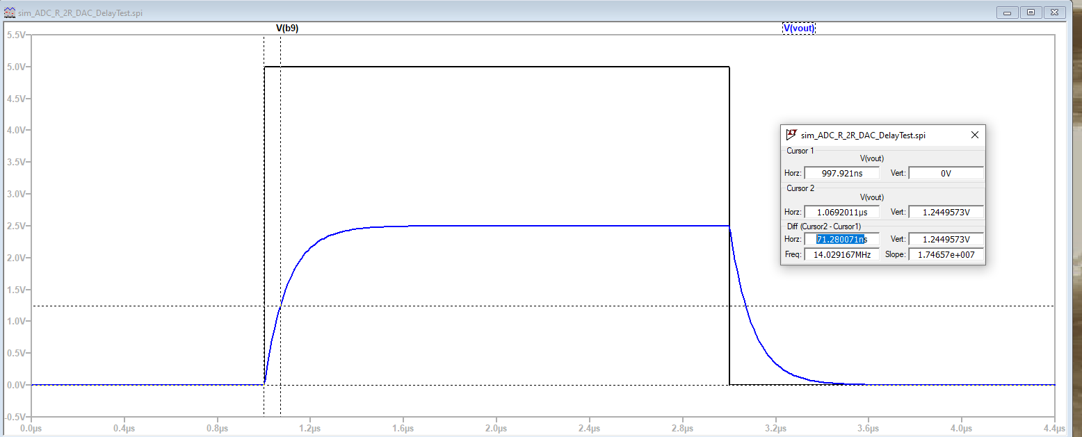
Figure 6. Time delay verfied as 70ns.
Discussion
This lab solidified how the R-2R DAC is implemented. VLSI takes some
getting used to again, but came back quickly as I worked through the
lab. Time delay verification further shows the properties of a
capacitor.