Task 1:
In this task we started by building and simulating the ring oscillator. This was built using an array of previously built inverters.
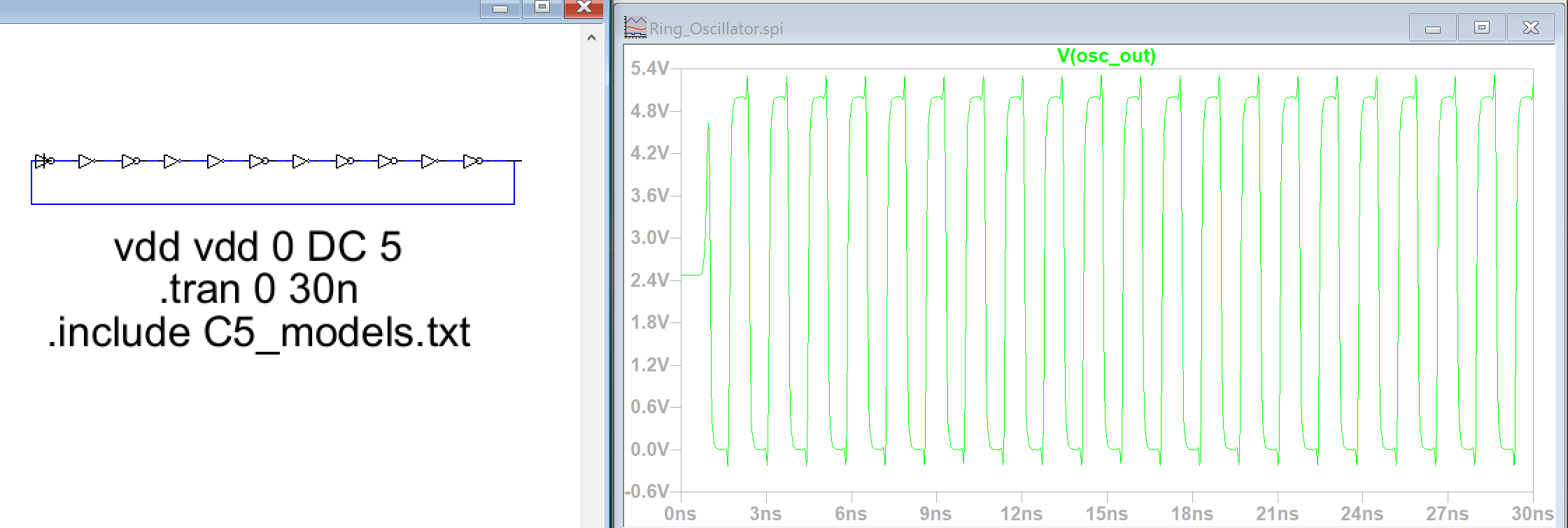
Figure 1: The schematic of the oscilator is built in Electric VLSI and it's output is displayed in LT Spice.
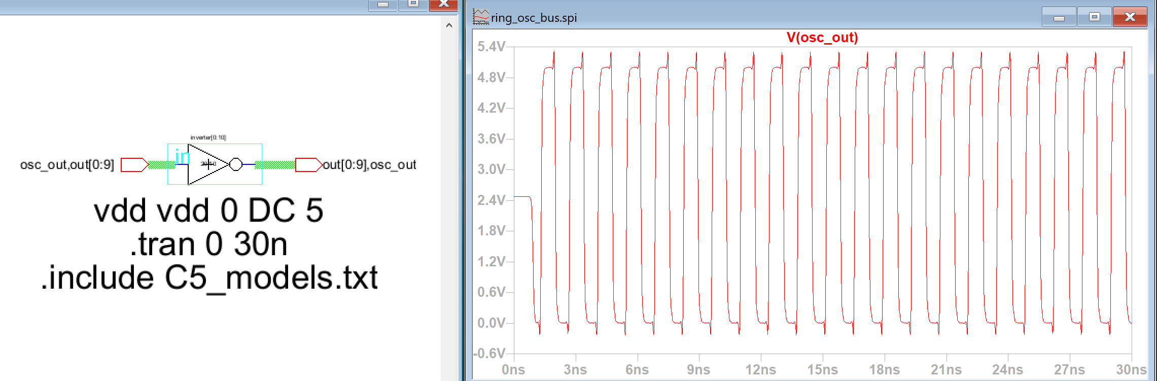
Figure 2: The schematic is recreated using the bus feature in Electric VLSI with it's output displayed in LT Spice.
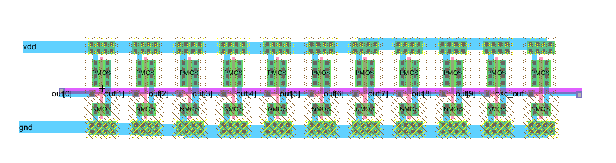
Figure 3: The layout of the oscillator is constructed.
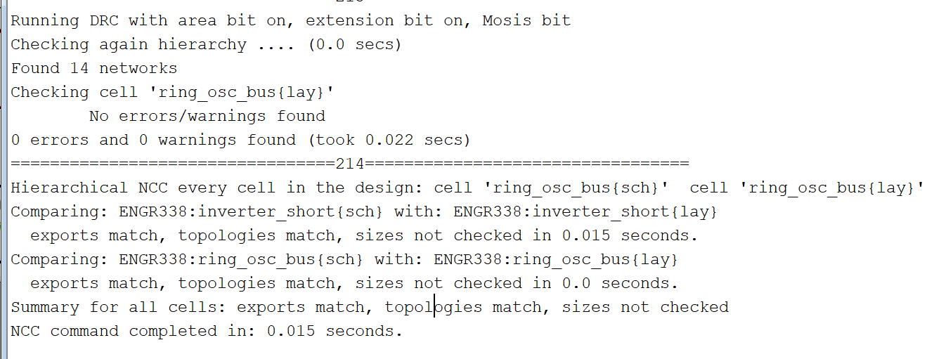
Figure 4: The layout passes both DRC and NCC error checks.
Task 2:
In this task we built an 8-bit AND gate starting with a standard AND gate.
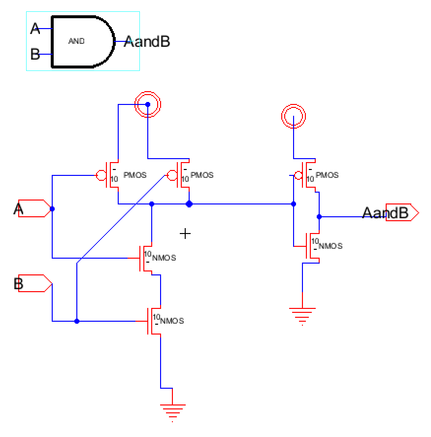
Figure 5: The schematic of the AND gate is built in Electric VLSI
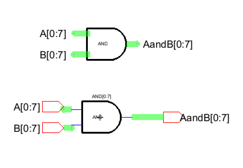
Figure 6: After the AND gate is built an array of 8 gates is created to make the 8-bit AND gate.
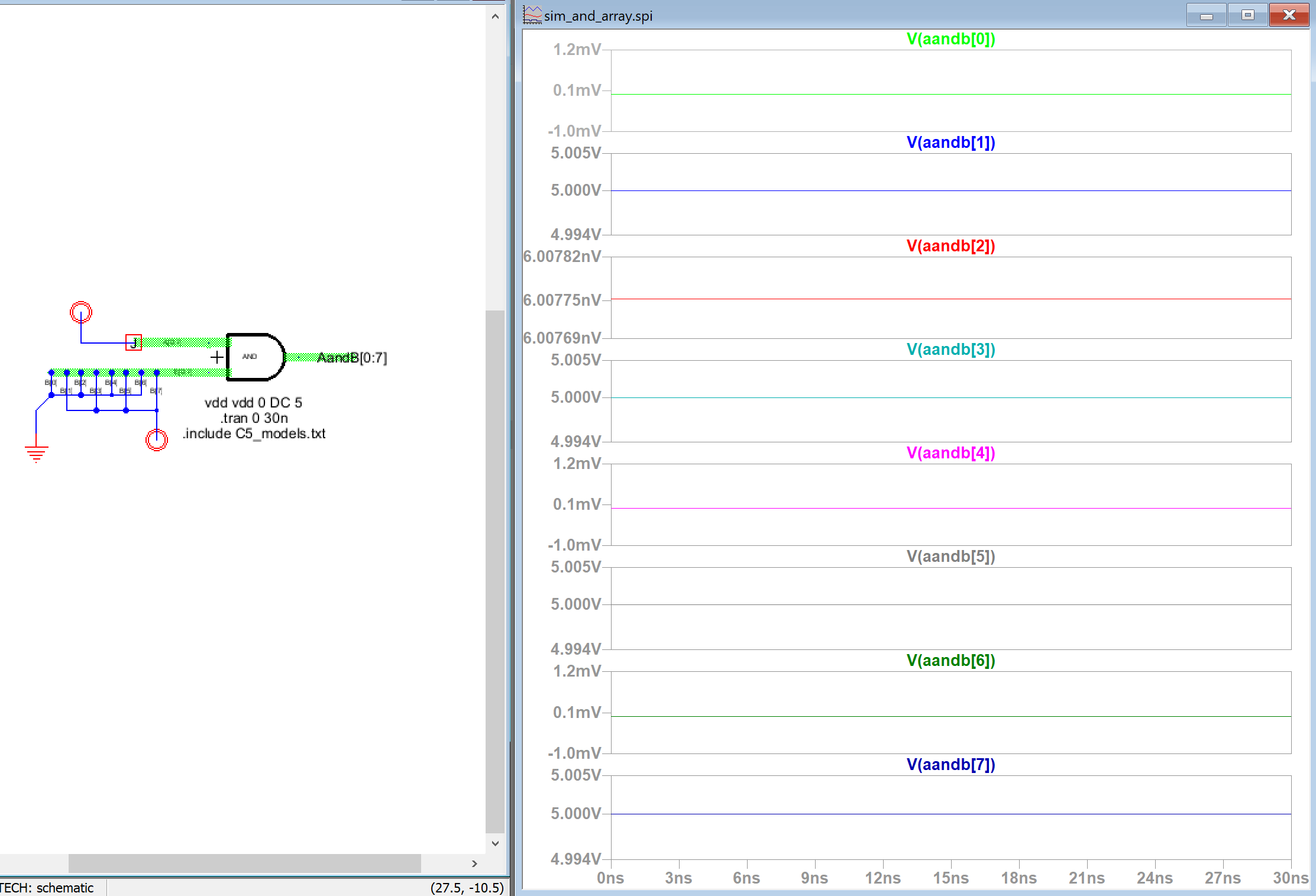
Figure 7: The functionality of the 8bit AND gate can then be tested using the above simulation.
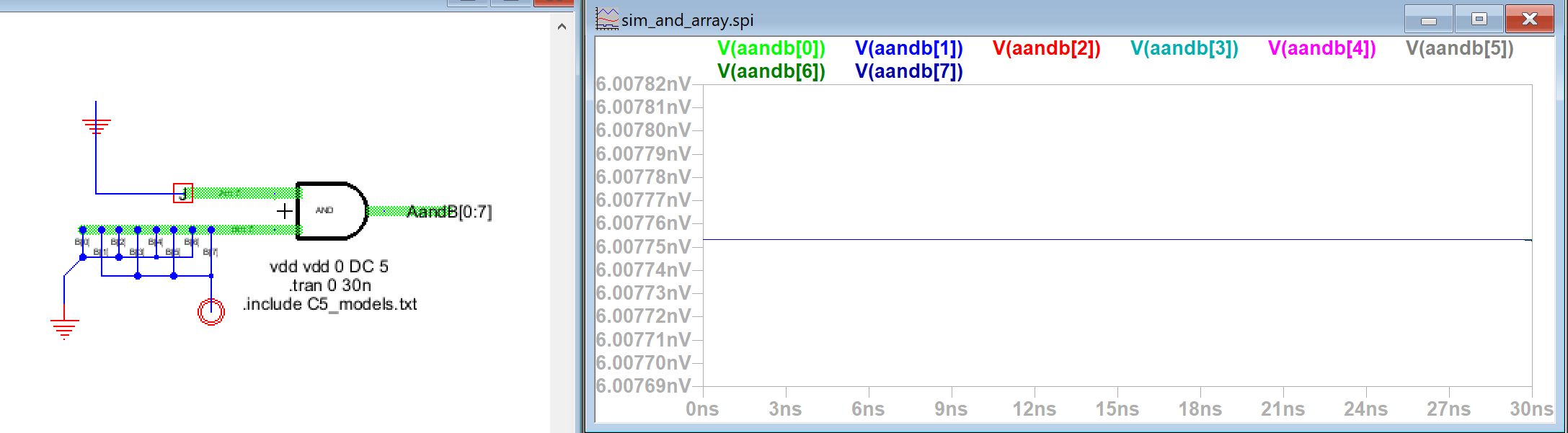
Figure 8: The functionality of the 8bit AND gate can then be tested further using the above simulation.
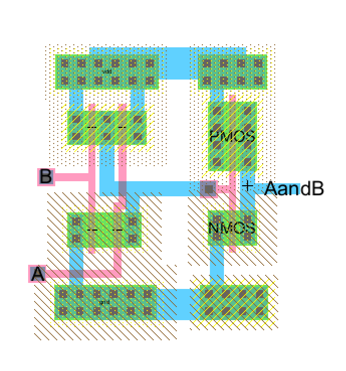
Figure 9: The layout of the AND gate is then built.
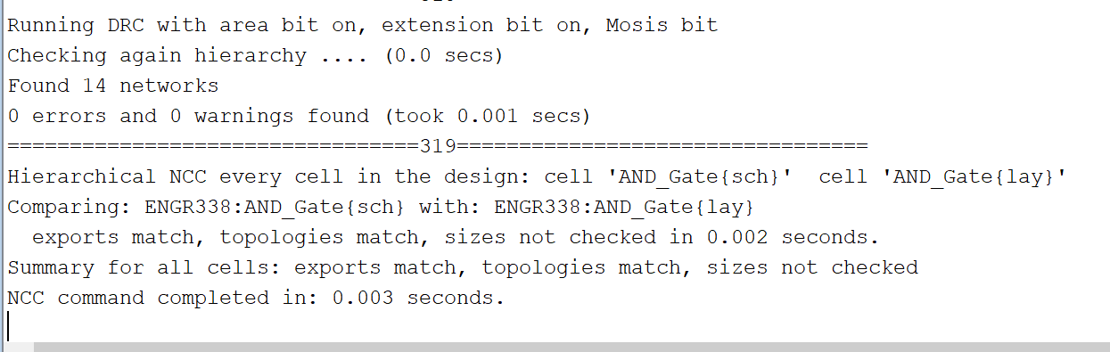
Figure 10: The layout passes both DRC and NCC error checks.
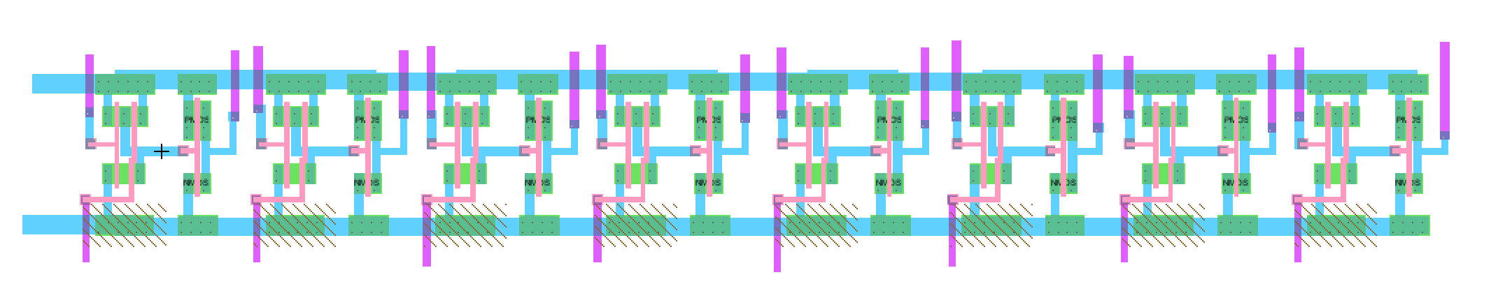
Figure 11: The layout of the array can then be built.
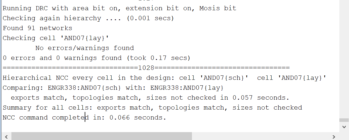
Figure 12: The layout of the 8bit AND array passes both DRC and NCC error checks.
Task 3:
In this task we built an 8-bit OR gate starting with a standard OR gate.
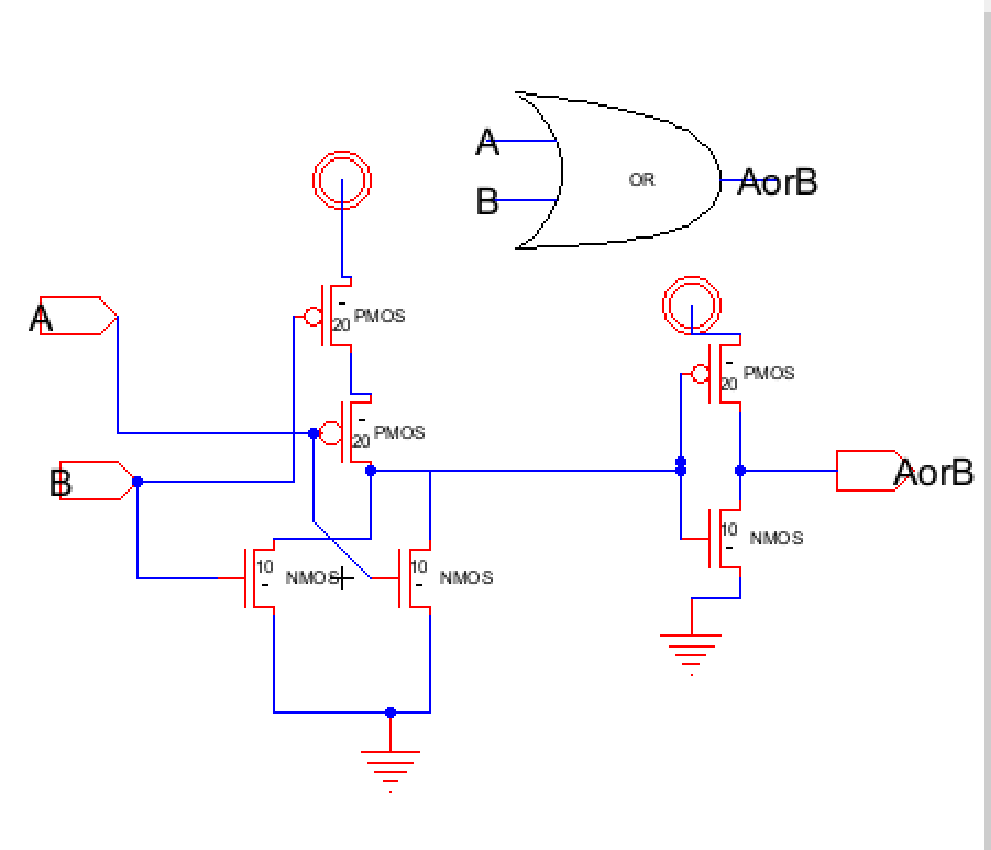
Figure 13: The schematic of the OR gate is built in Electric VLSI
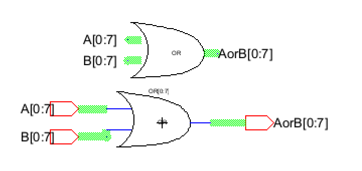
Figure 14: After the OR gate is built an array of 8 gates is created to make the 8-bit OR gate.
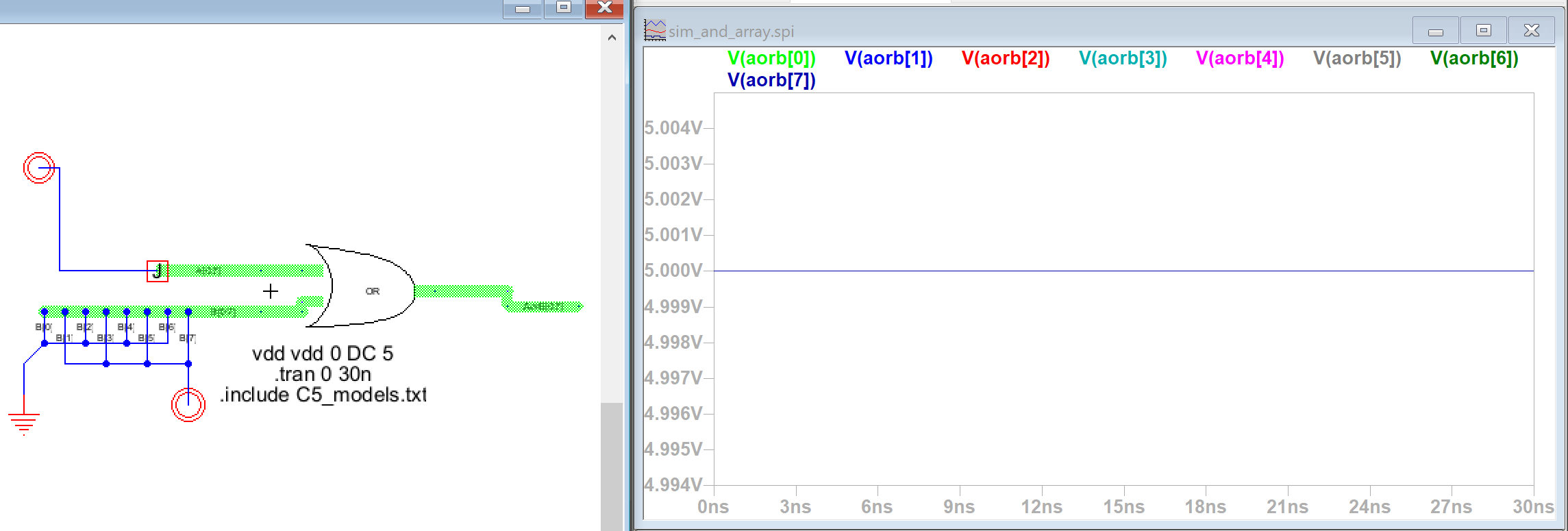
Figure 15: The functionality of the 8bit OR gate can then be tested using the above simulation.
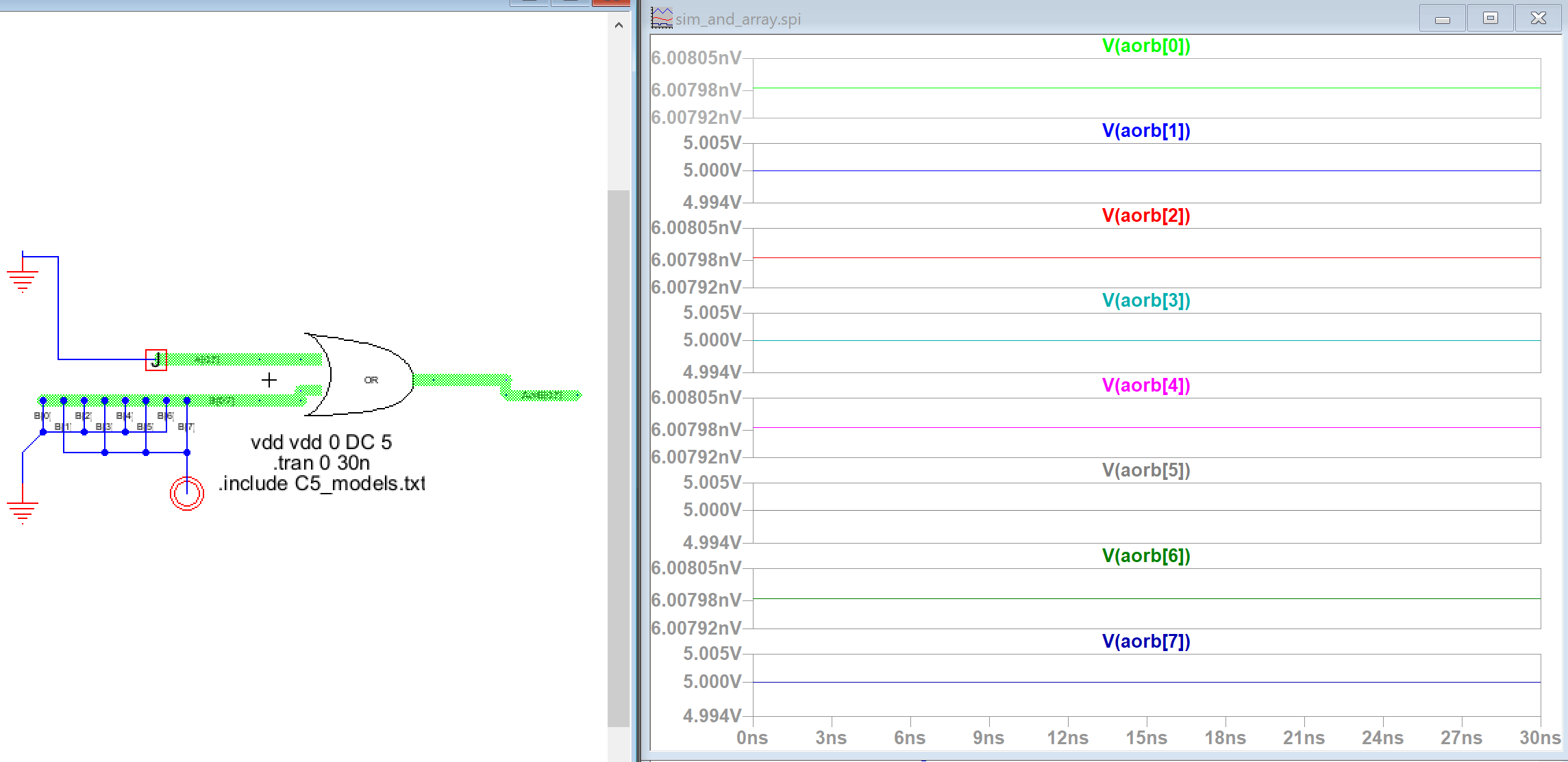
Figure 16: The functionality of the 8bit OR gate can then be tested further using the above simulation.
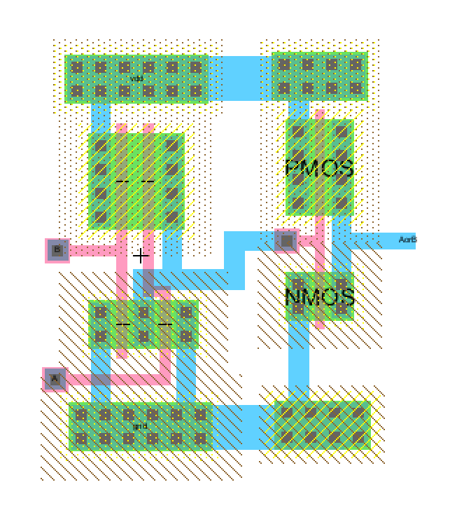
Figure 17: The layout of the OR gate is then built.
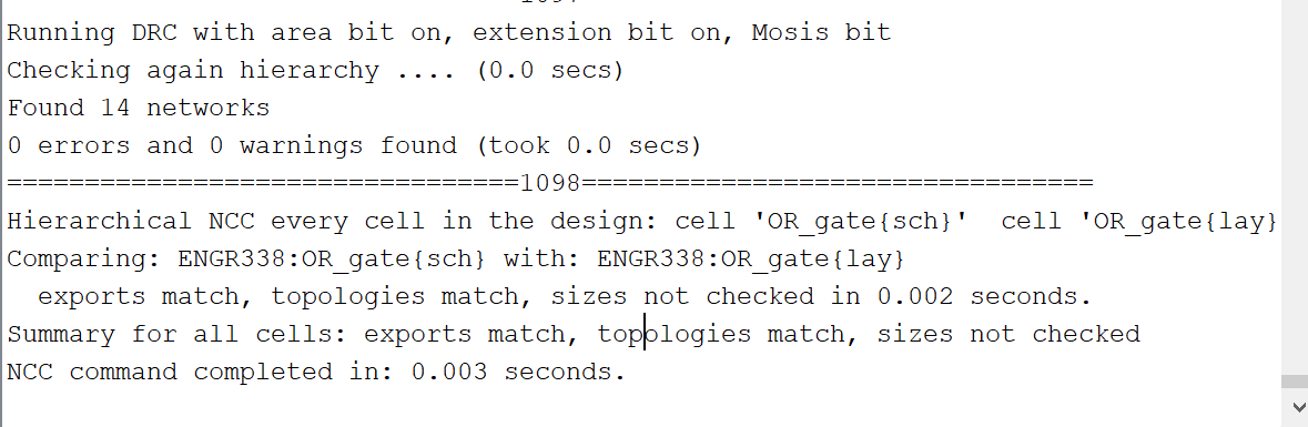
Figure 18: The layout passes both DRC and NCC error checks.
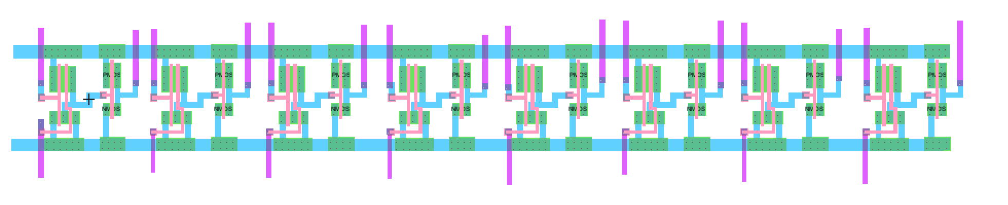
Figure 19: The layout of the array can then be built.
Task 5:
In this task we built an 8bit NOR gate using the previously built XOR gate.
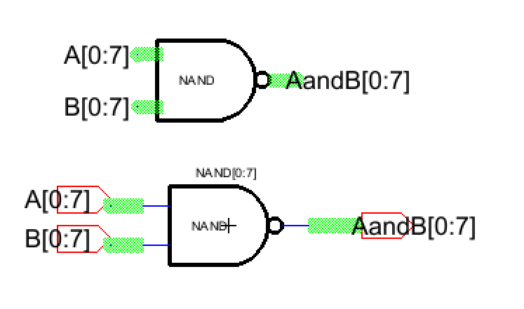
Figure 26: The 8bit array of NOR gates is built.
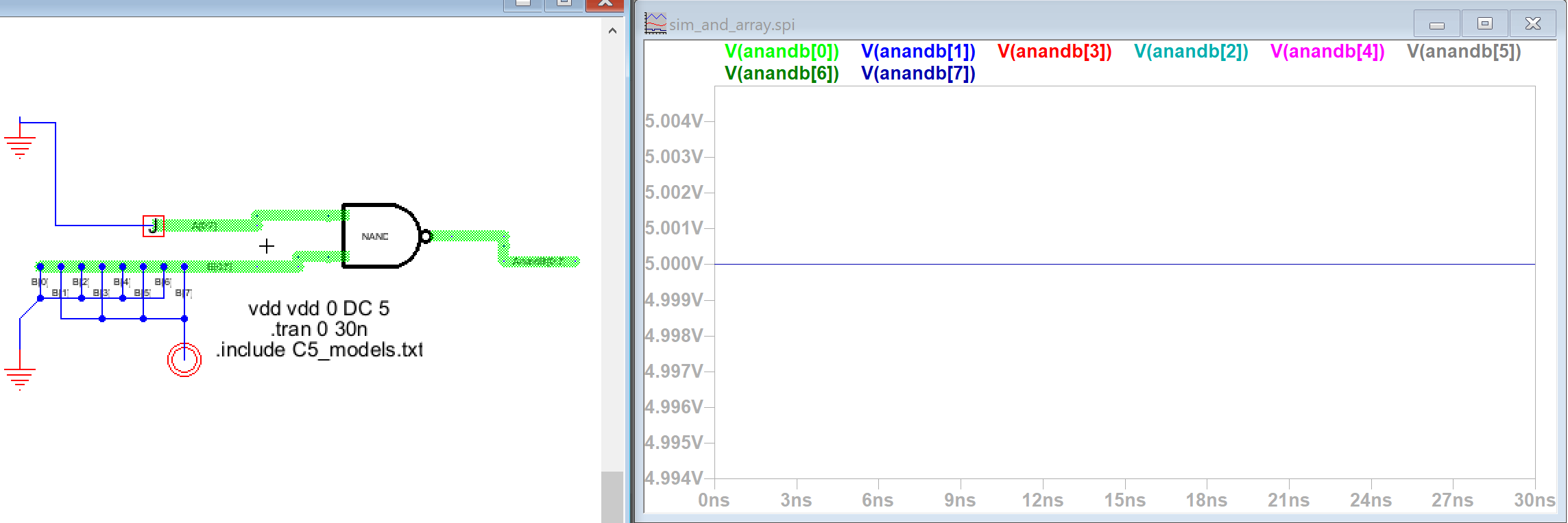
Figure 27: The functionality of the 8bit NOR gate can then be tested using the above simulation.
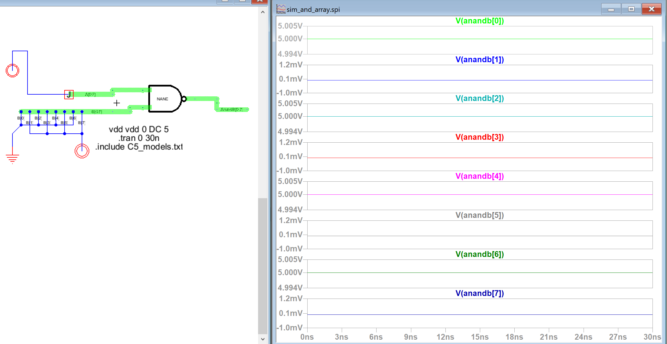
Figure 28: The functionality of the 8bit NOR gate can then be tested further using the above simulation.
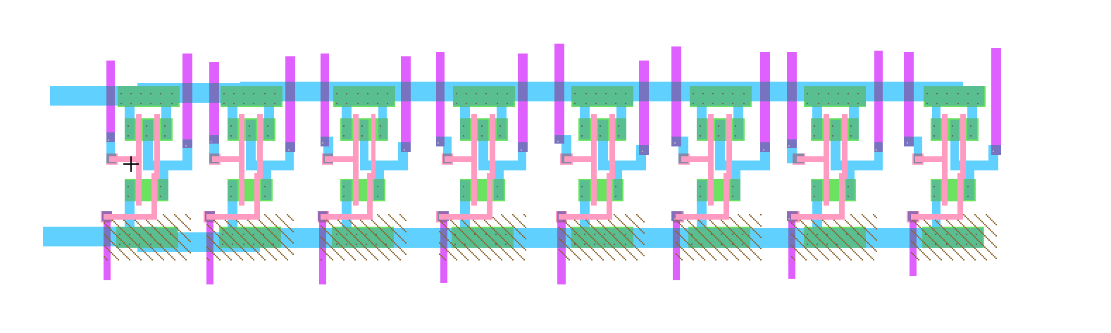
Figure 29: The layout of the array can then be built.
Discussion:In this task we started by building and simulating the ring oscillator. This was built using an array of previously built inverters.
Figure 1: The schematic of the oscilator is built in Electric VLSI and it's output is displayed in LT Spice.
Figure 2: The schematic is recreated using the bus feature in Electric VLSI with it's output displayed in LT Spice.
Figure 3: The layout of the oscillator is constructed.
Figure 4: The layout passes both DRC and NCC error checks.
Task 2:
In this task we built an 8-bit AND gate starting with a standard AND gate.
Figure 5: The schematic of the AND gate is built in Electric VLSI
Figure 6: After the AND gate is built an array of 8 gates is created to make the 8-bit AND gate.
Figure 7: The functionality of the 8bit AND gate can then be tested using the above simulation.
Figure 8: The functionality of the 8bit AND gate can then be tested further using the above simulation.
Figure 9: The layout of the AND gate is then built.
Figure 10: The layout passes both DRC and NCC error checks.
Figure 11: The layout of the array can then be built.
Figure 12: The layout of the 8bit AND array passes both DRC and NCC error checks.
Task 3:
In this task we built an 8-bit OR gate starting with a standard OR gate.
Figure 13: The schematic of the OR gate is built in Electric VLSI
Figure 14: After the OR gate is built an array of 8 gates is created to make the 8-bit OR gate.
Figure 15: The functionality of the 8bit OR gate can then be tested using the above simulation.
Figure 16: The functionality of the 8bit OR gate can then be tested further using the above simulation.
Figure 17: The layout of the OR gate is then built.
Figure 18: The layout passes both DRC and NCC error checks.
Figure 19: The layout of the array can then be built.
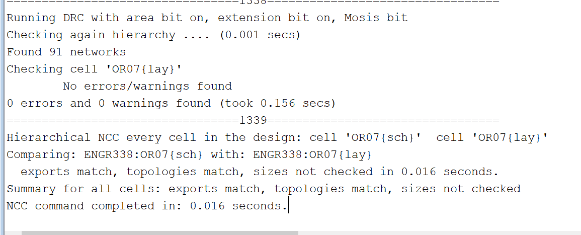
Figure 20: The layout of the 8bit OR array passes both DRC and NCC error checks.
Task 4:
In this task we built an 8bit NAND gate using the previously built NAND gate.
Figure 21: The 8bit array of NAND gates is built.
Figure 22: The functionality of the 8bit NAND gate can then be tested using the above simulation.
Figure 23: The functionality of the 8bit NAND gate can then be tested further using the above simulation.
Figure 24: The layout of the array can then be built.
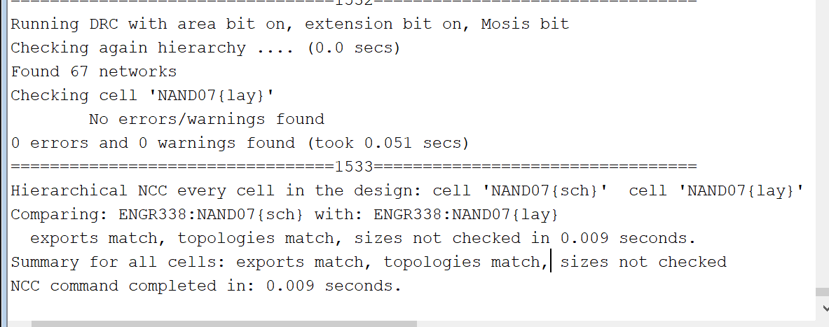
Figure 25: The layout of the 8bit NAND array passes both DRC and NCC error checks.
Task 5:
In this task we built an 8bit NOR gate using the previously built XOR gate.
Figure 26: The 8bit array of NOR gates is built.
Figure 27: The functionality of the 8bit NOR gate can then be tested using the above simulation.
Figure 28: The functionality of the 8bit NOR gate can then be tested further using the above simulation.
Figure 29: The layout of the array can then be built.
Figure 30: The layout of the 8bit NOR array passes both DRC and NCC error checks.
This lab was an excellent overview of the internal design of ring oscillator and multibit gates. This lab helped to show how the internal structure of these devices and how they are designed using the bus feature in Electric VLSI.