Task 1:
In this task we started by building the NAND gate schematic in Electric VLSI and then testing its output in LT Spice. The layout of the gate was then created in Electric VLSI and checked for errors.
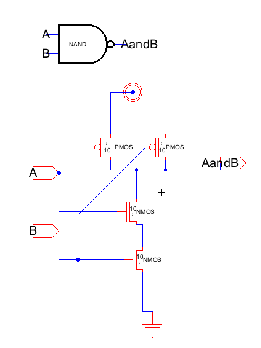
Figure 1: The schematic and icon view of the NAND gate.
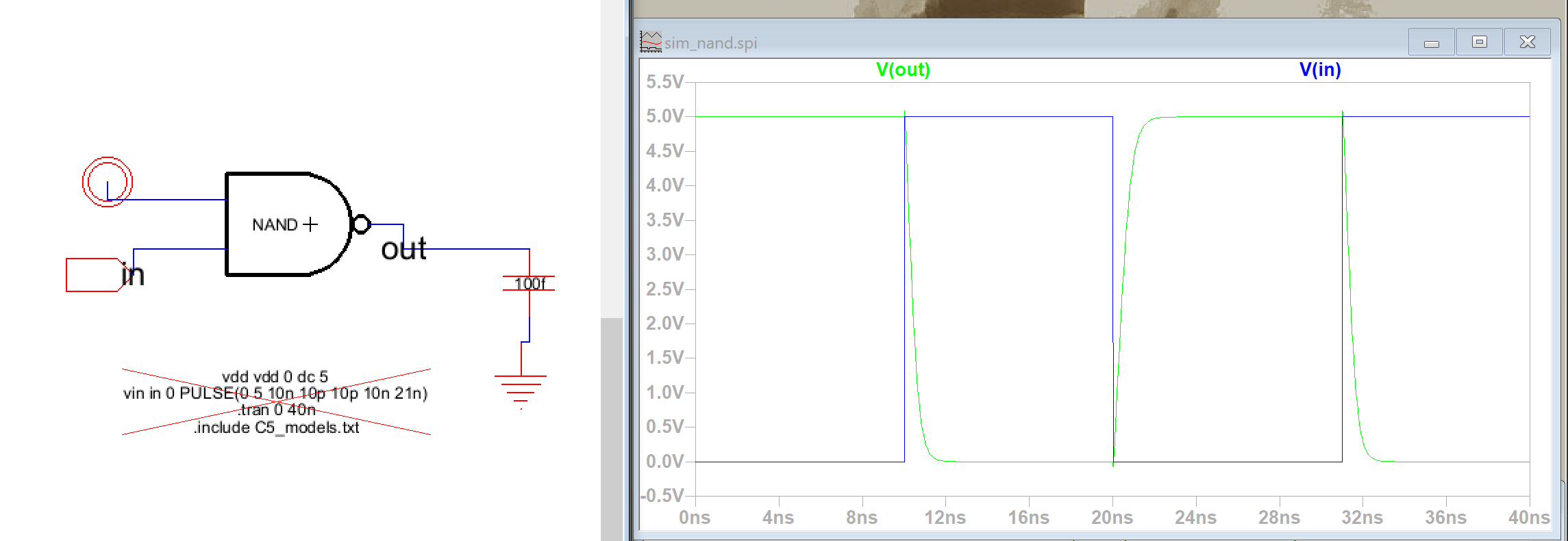
Figure 2: The NAND gate is used to drive a 100fF capacitor and the output is plotted in LT Spice.
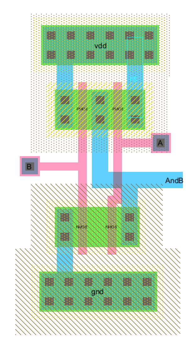
Figure 3: The NAND gate is constructed using the layout view.
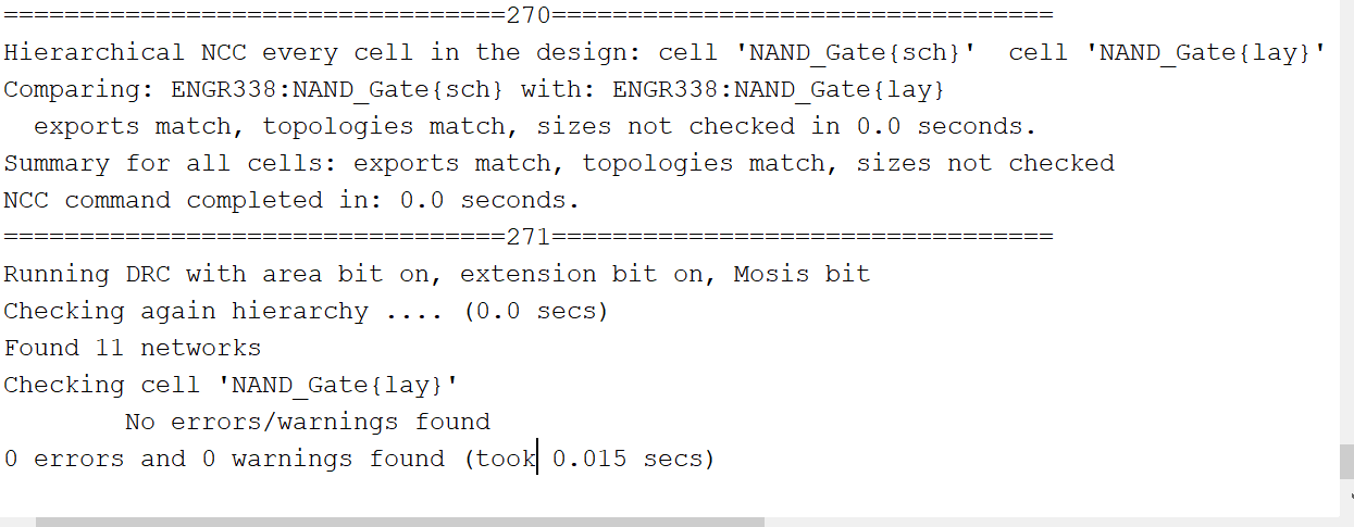
Figure 4: The final NAND layout and schematic both pass the DRC and NCC error checks.
Task 2:
In this task we built the NOR gate schematic in Electric VLSI and then tested it's output in LT Spice. The layout of the gate was then created in Electric VLSI and checked for errors.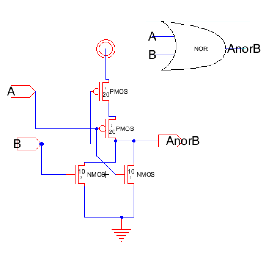
Figure 5: The schematic and icon view of the NOR gate.
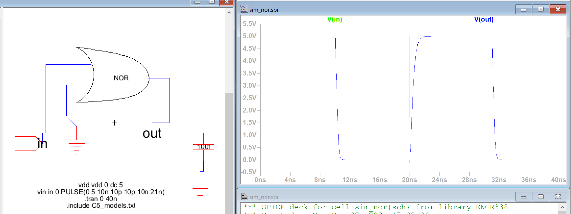
Figure 6: The NOR gate is used to drive a 100fF capacitor and the output is plotted in LT Spice.
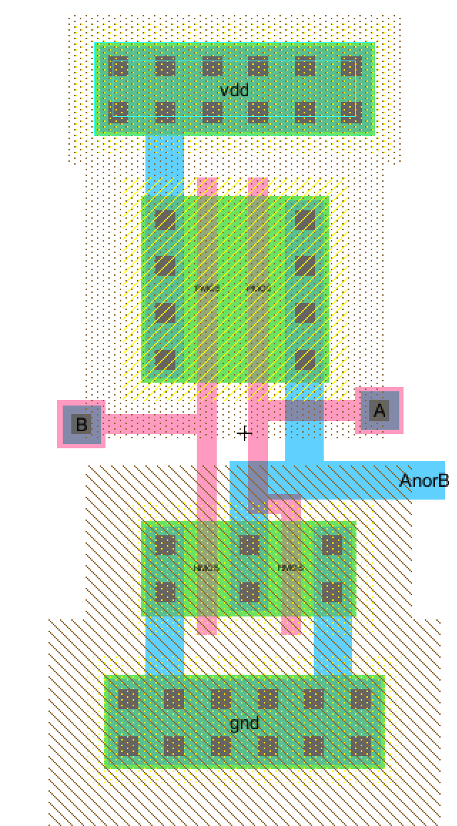
Figure 7: The NOR gate is constructed using the layout view.
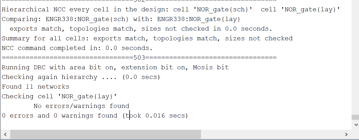
Figure 8: The final NOR layout and schematic both pass the DRC and NCC error checks.
Task 3:
In this task we built the XOR gate schematic in Electric VLSI and then tested it's output in LT Spice. The layout of the gate was then created in Electric VLSI and checked for errors.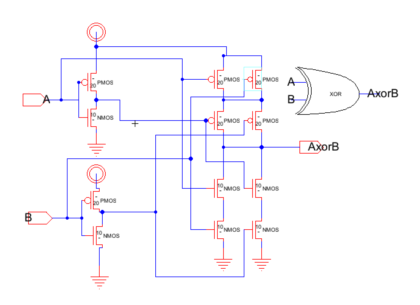
Figure 9: The schematic and icon view of the XOR gate.
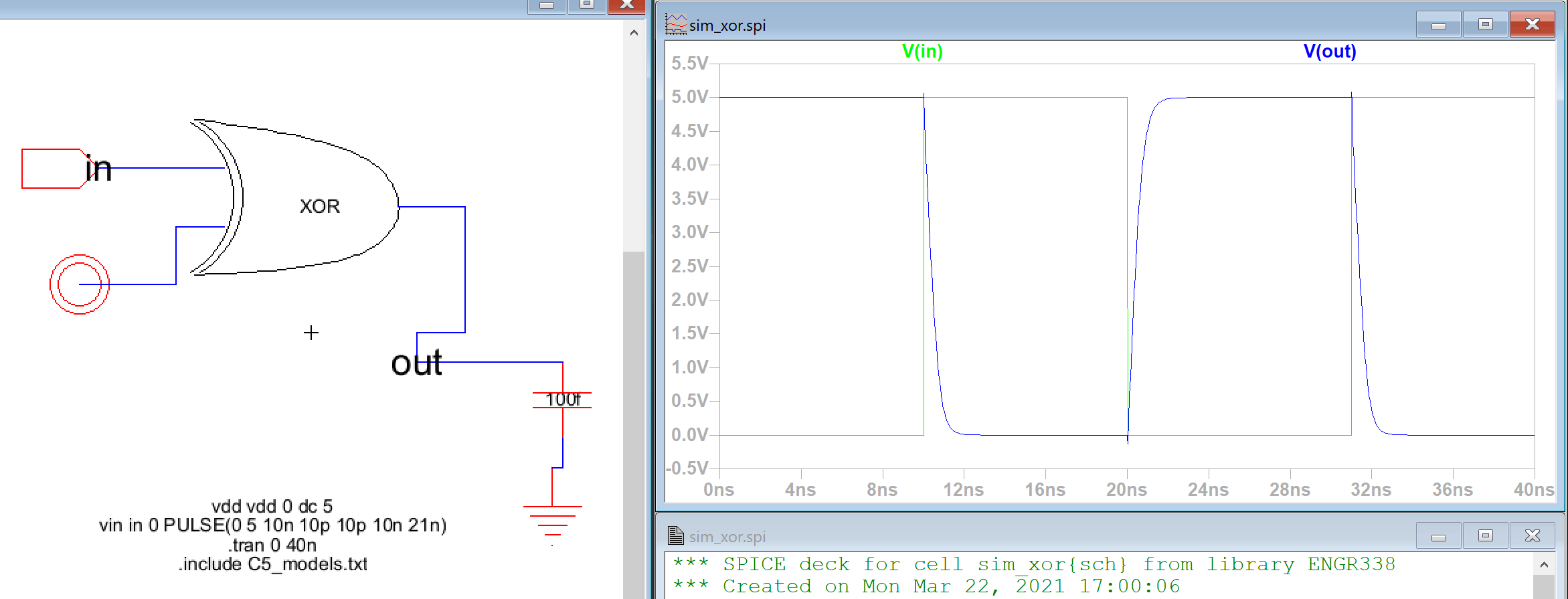
Figure 10: The XOR gate is used to drive a 100fF capacitor and the output is plotted in LT Spice.
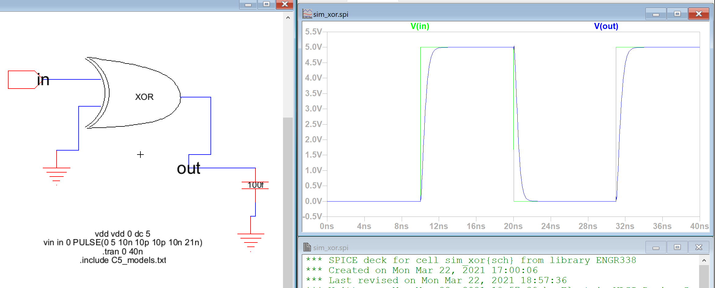
Figure 11: The XOR gate is used to drive a 100fF capacitor and the output is plotted in LT Spice.
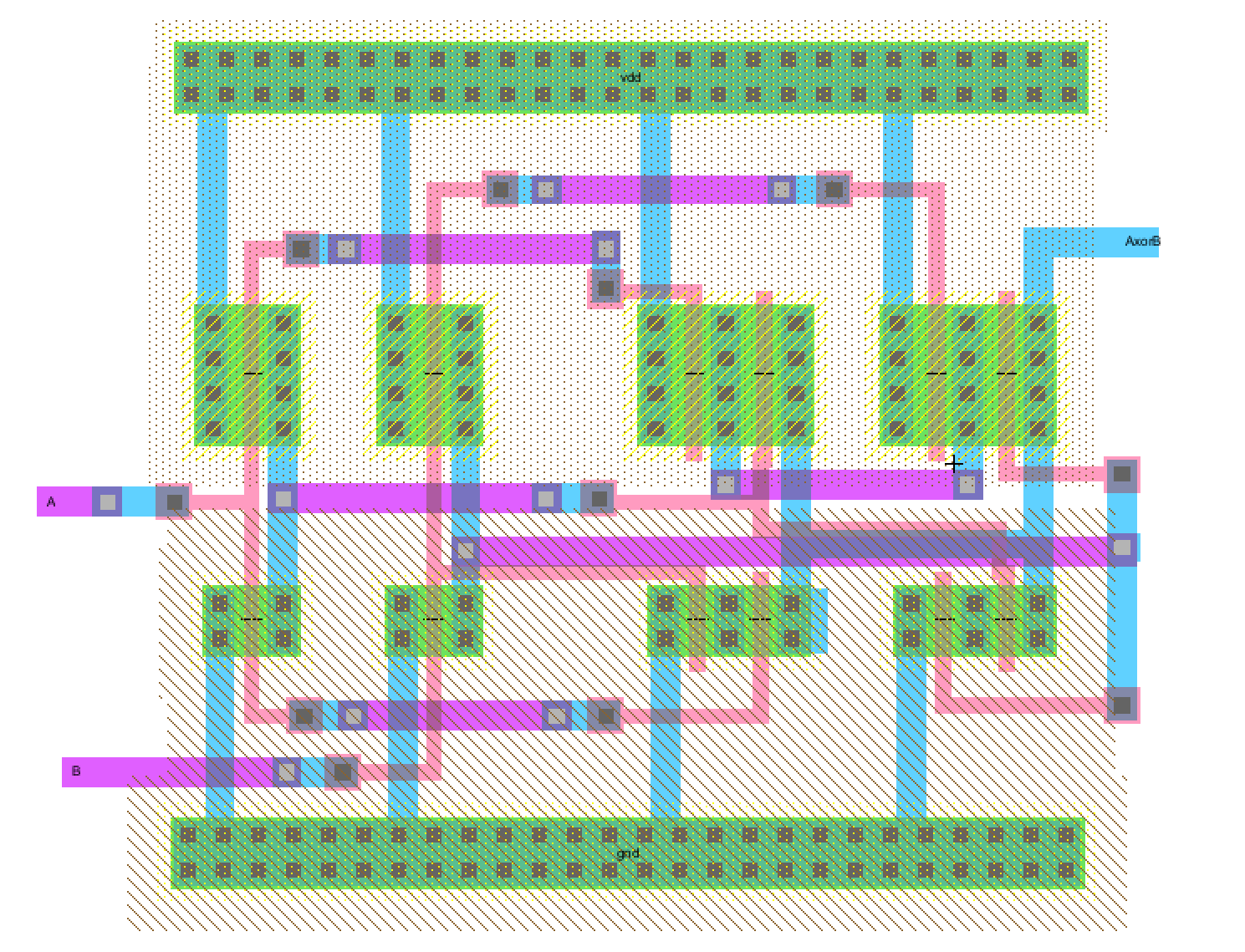
Figure 12: The XOR gate is constructed using the layout view.
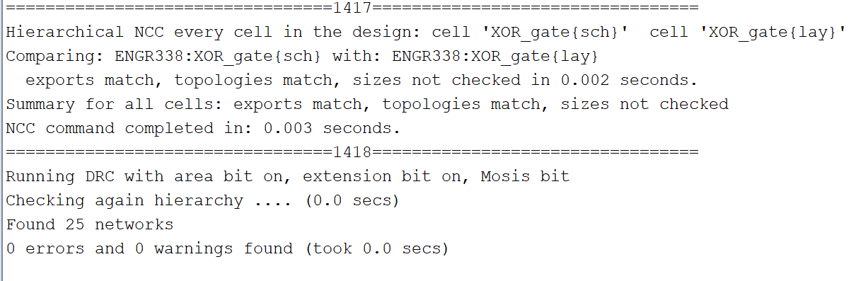
Figure 13: The final XOR layout and schematic both pass the DRC and NCC error checks.
Task 4:
In this task we built the Full Adder schematic in Electric VLSI and then tested it's output in LT Spice. The layout of the Full Adder was then created in Electric VLSI and checked for errors.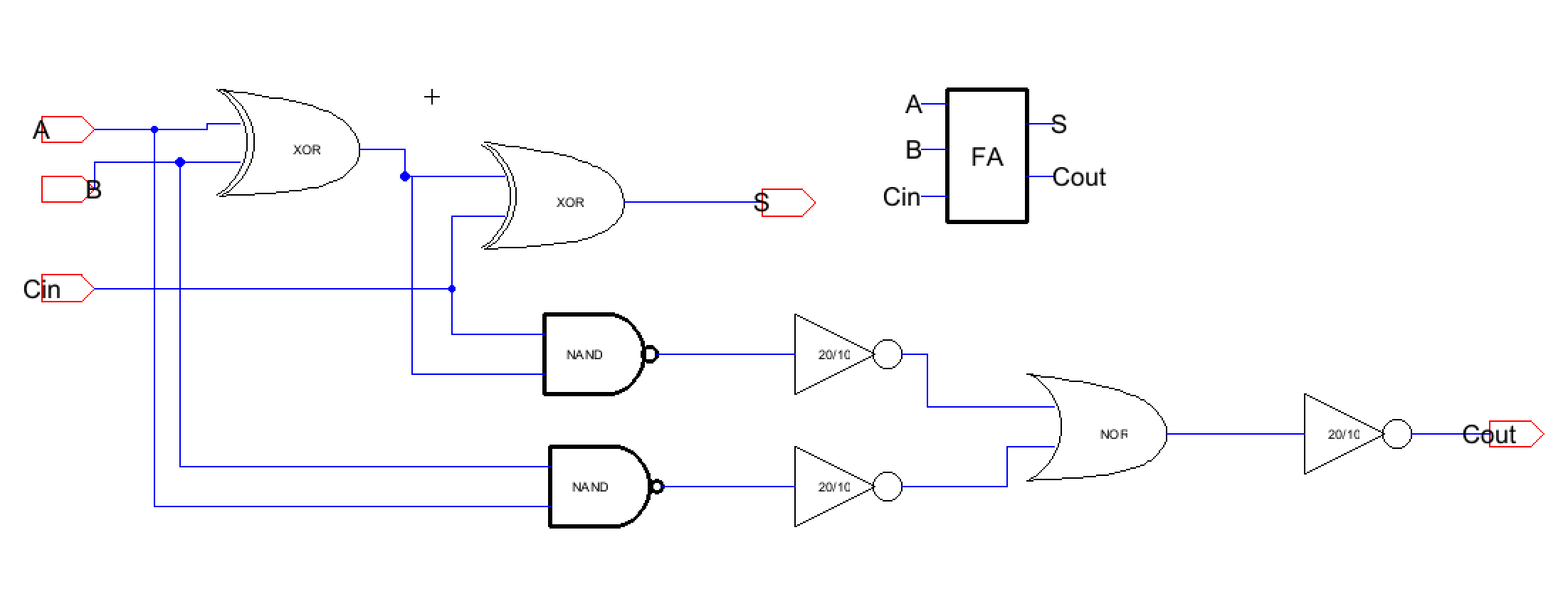
Figure 14: The schematic and icon view of the Full Adder.
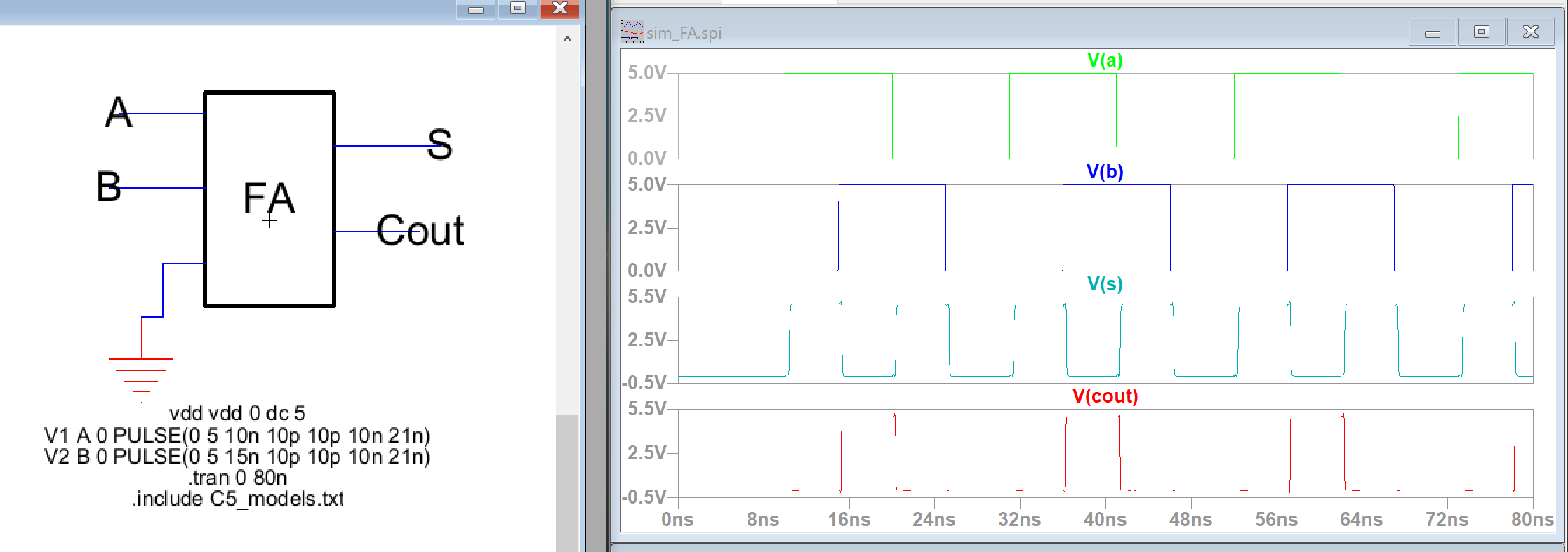
Figure 15: The output of the Full Adder is plotted in LT Spice
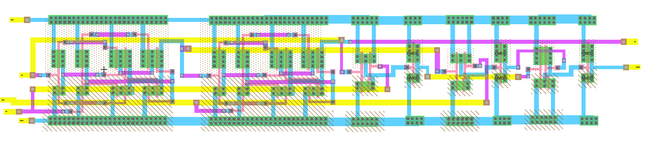
Figure 16: The Full Adder is constructed using the layout view.
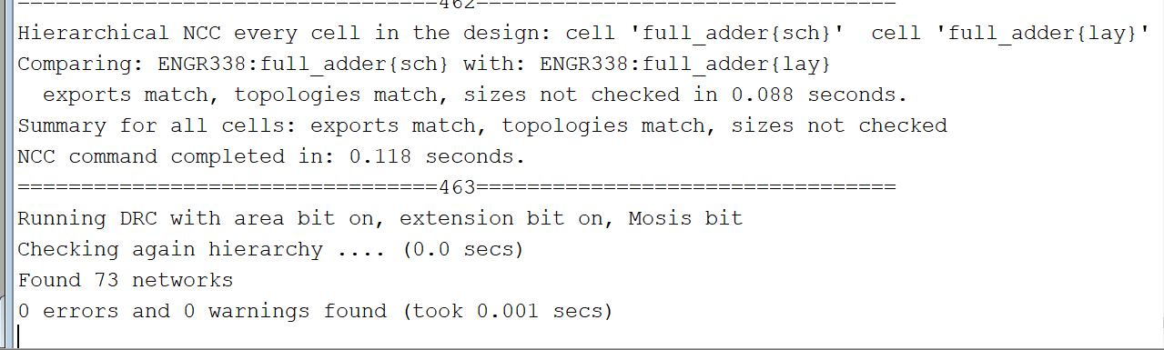
Figure 17: The final Full Adder layout and schematic both pass the DRC and NCC error checks.
In this task we started by building the NAND gate schematic in Electric VLSI and then testing its output in LT Spice. The layout of the gate was then created in Electric VLSI and checked for errors.
Figure 1: The schematic and icon view of the NAND gate.
Figure 2: The NAND gate is used to drive a 100fF capacitor and the output is plotted in LT Spice.
Figure 3: The NAND gate is constructed using the layout view.
Figure 4: The final NAND layout and schematic both pass the DRC and NCC error checks.
Task 2:
In this task we built the NOR gate schematic in Electric VLSI and then tested it's output in LT Spice. The layout of the gate was then created in Electric VLSI and checked for errors.
Figure 5: The schematic and icon view of the NOR gate.
Figure 6: The NOR gate is used to drive a 100fF capacitor and the output is plotted in LT Spice.
Figure 7: The NOR gate is constructed using the layout view.
Figure 8: The final NOR layout and schematic both pass the DRC and NCC error checks.
Task 3:
In this task we built the XOR gate schematic in Electric VLSI and then tested it's output in LT Spice. The layout of the gate was then created in Electric VLSI and checked for errors.
Figure 9: The schematic and icon view of the XOR gate.
Figure 10: The XOR gate is used to drive a 100fF capacitor and the output is plotted in LT Spice.
Figure 11: The XOR gate is used to drive a 100fF capacitor and the output is plotted in LT Spice.
Figure 12: The XOR gate is constructed using the layout view.
Figure 13: The final XOR layout and schematic both pass the DRC and NCC error checks.
Task 4:
In this task we built the Full Adder schematic in Electric VLSI and then tested it's output in LT Spice. The layout of the Full Adder was then created in Electric VLSI and checked for errors.
Figure 14: The schematic and icon view of the Full Adder.
Figure 15: The output of the Full Adder is plotted in LT Spice
Figure 16: The Full Adder is constructed using the layout view.
Figure 17: The final Full Adder layout and schematic both pass the DRC and NCC error checks.