Task 1:
In this task we created a schematic of the inverter using Electric VLSI
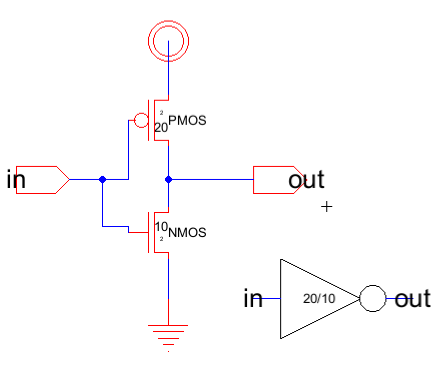
Figure 1. The schematic of the inverter is created using the PMOS and NMOS transistors.
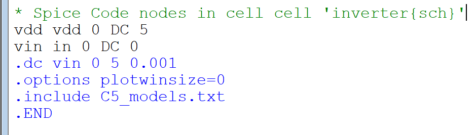
Figure 2. Spice code is added to the iverter to ensure the input is inverted.
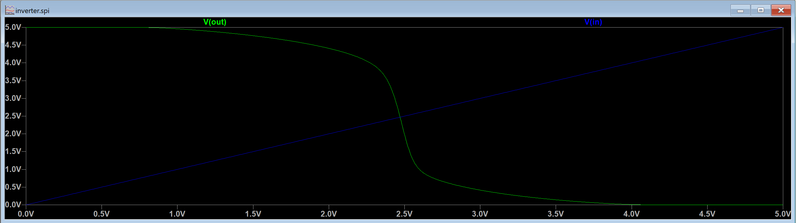
Figure 3. The output from LT Spice is plotted.
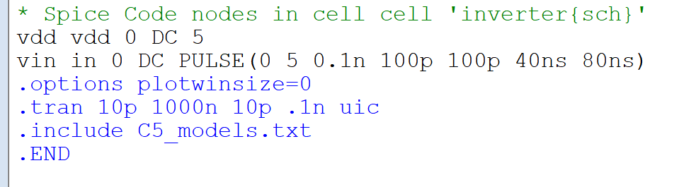
Figure 4. More LT Spice code is added to simulate a pulse wave input.
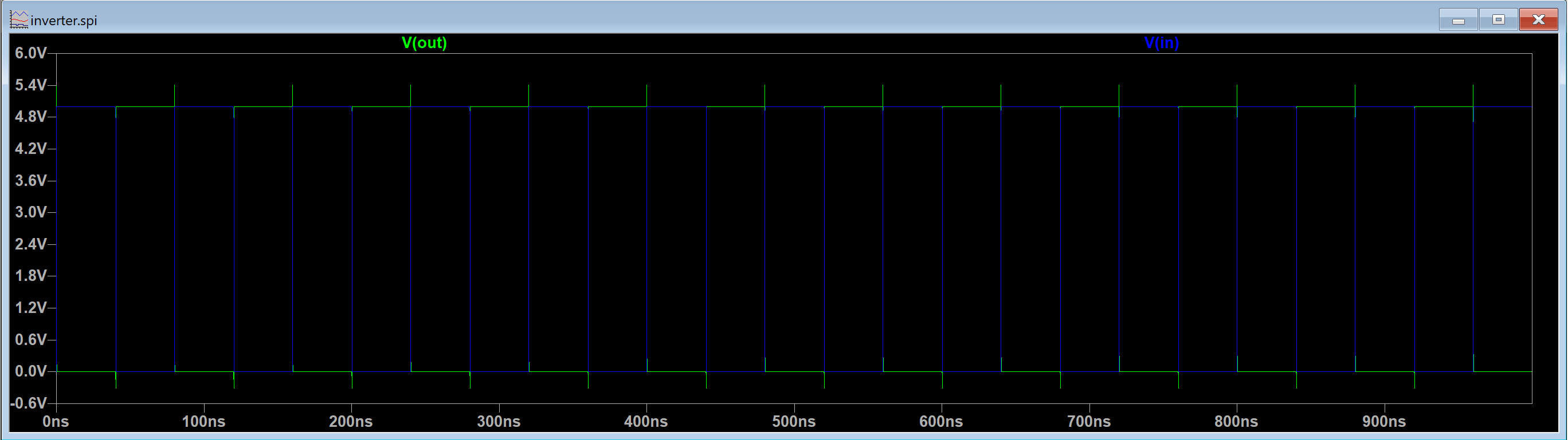
Figure 5. The output from LT Spice is plotted above.
Task 2:
In this task we created the layout of the inverter in Electric VLSI.
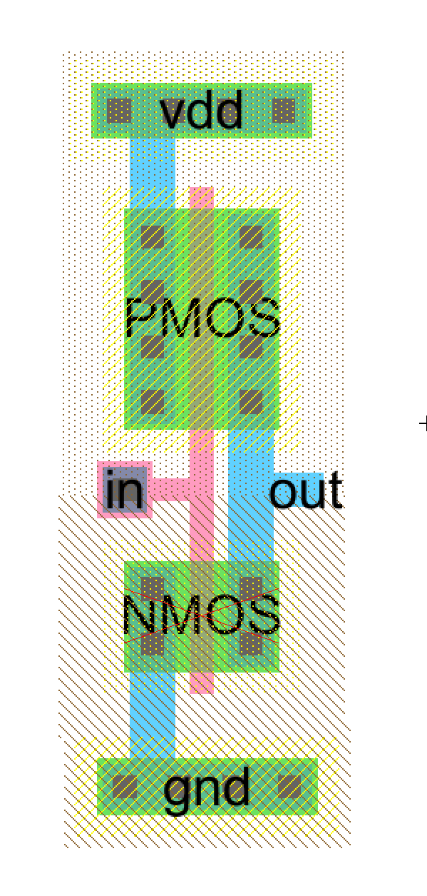
Figure 6. The layout of the inverter using both PMOS and NMOS transistors.
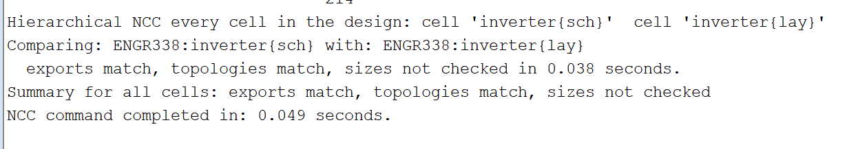
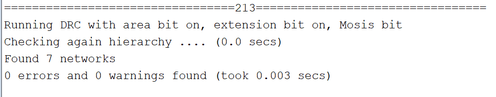
Figure 7. The inverter layout and schematic pass the NCC and DRC error checks.
Task 3:
In this task we used the multipler function in Electric VLSI to build a larger inverter. The previous inverter built was a 20/5-10/5 inverter while in this task we will create a 100/2-50/2 inverter.
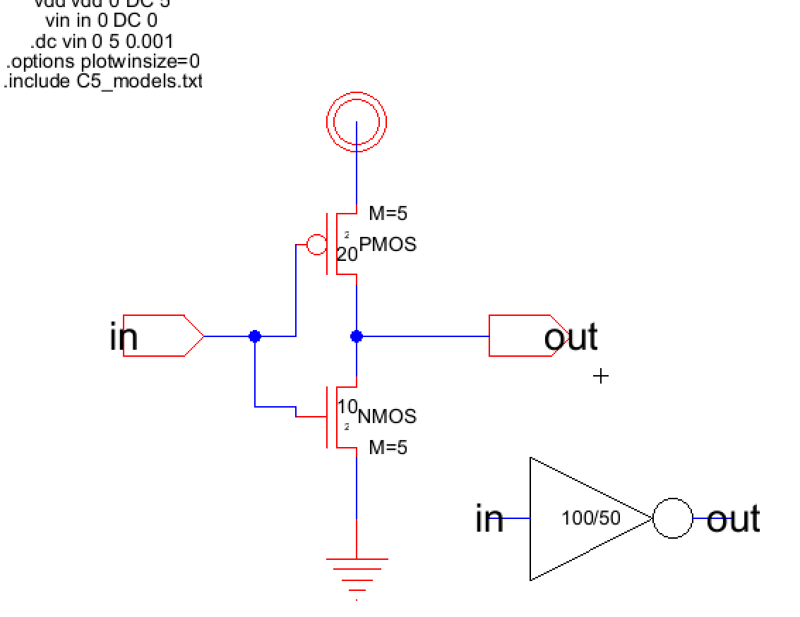
Figure 8. The schematic of our previous inverter is duplicated and edited to accommodate for the larger size inverter.
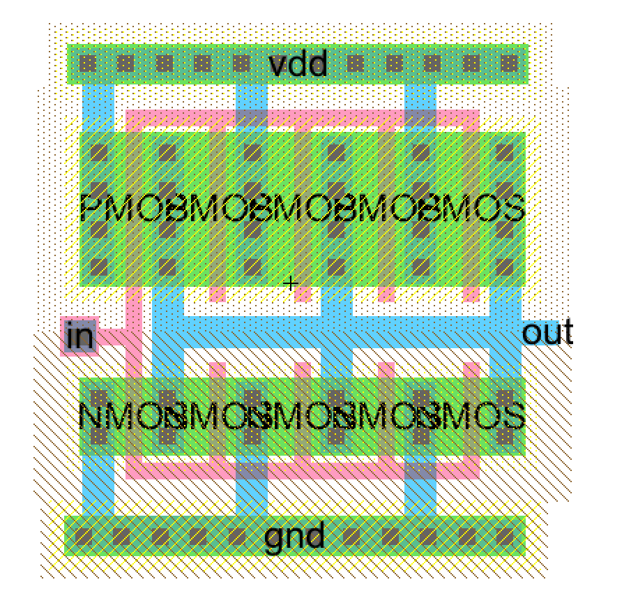
Figure 9. PMOS and NMOS are connected in parallel to create a larger inverter.
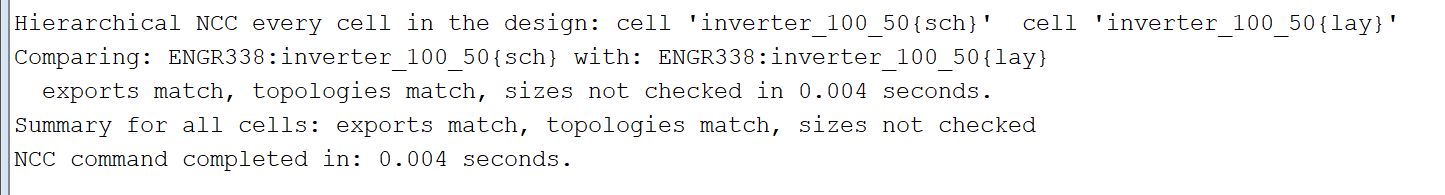
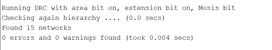
Figure 9. The schematic and layout of the larger inverter passed both NCC and DRC error checks.
Task 4:
In this task we ran simulations in LT Spice to verify the driving capability of the two inverters. Both the inverters are connected to a 100fF, 1pF, and a 10pF capacitor and the output is graphed in LT Spice.
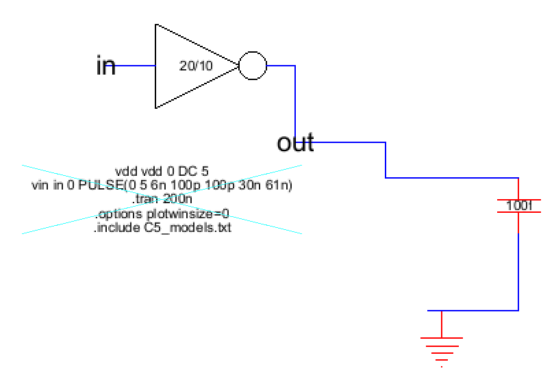
Figure 10. The 20/10 inverter is connected to a 100fF capacitor.
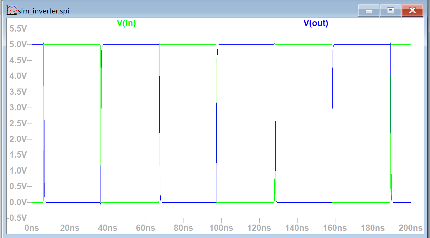
Figure 11. The input of the inverter and the output is graphed above.
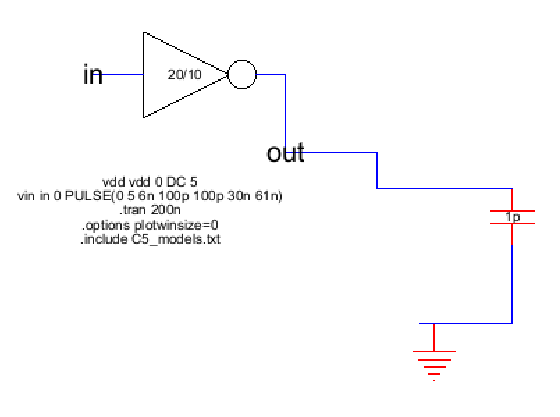
Figure 12. The 20/10 inverter is connected to a 1pF capacitor.
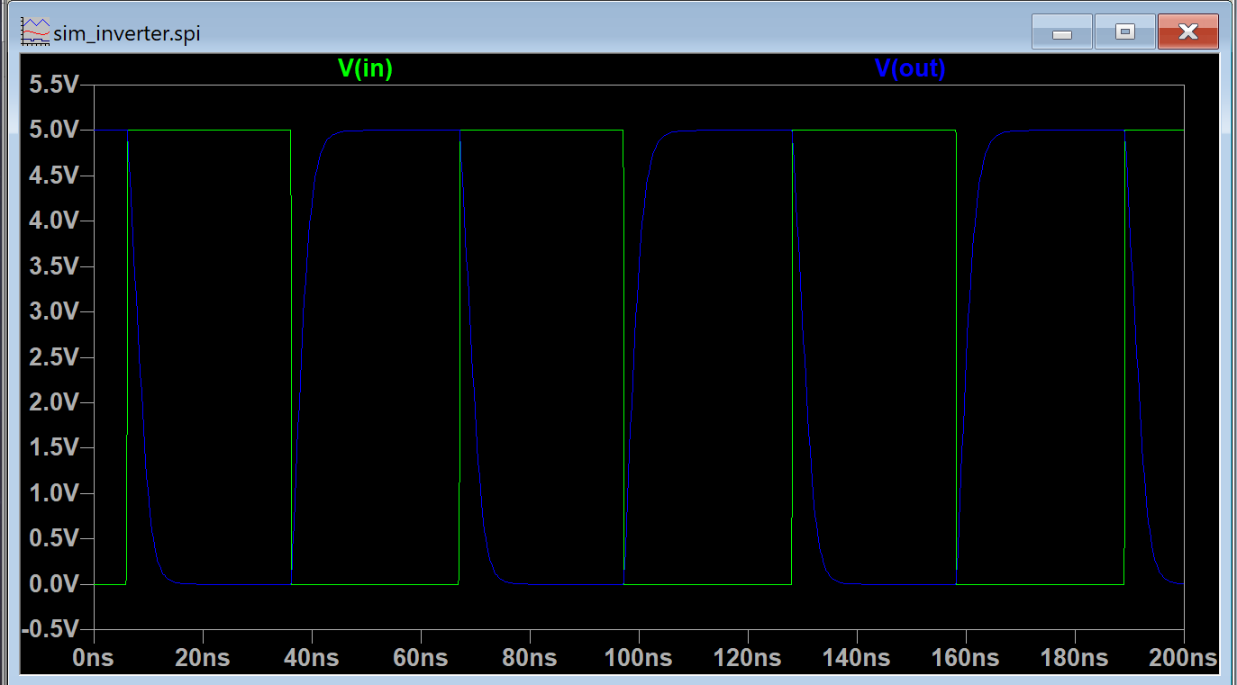
Figure 13. The input of the inverter and the output is graphed above.
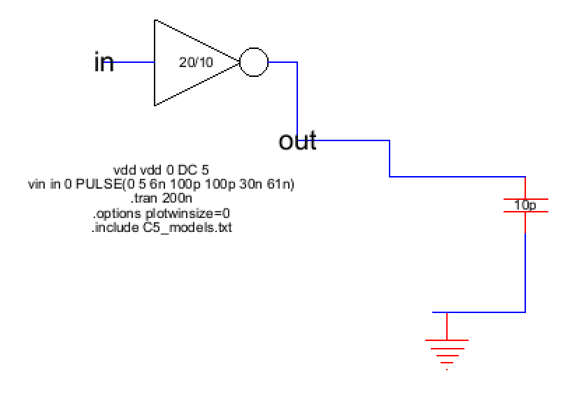
Figure 14. The 20/10 inverter is connected to a 10pF capacitor.
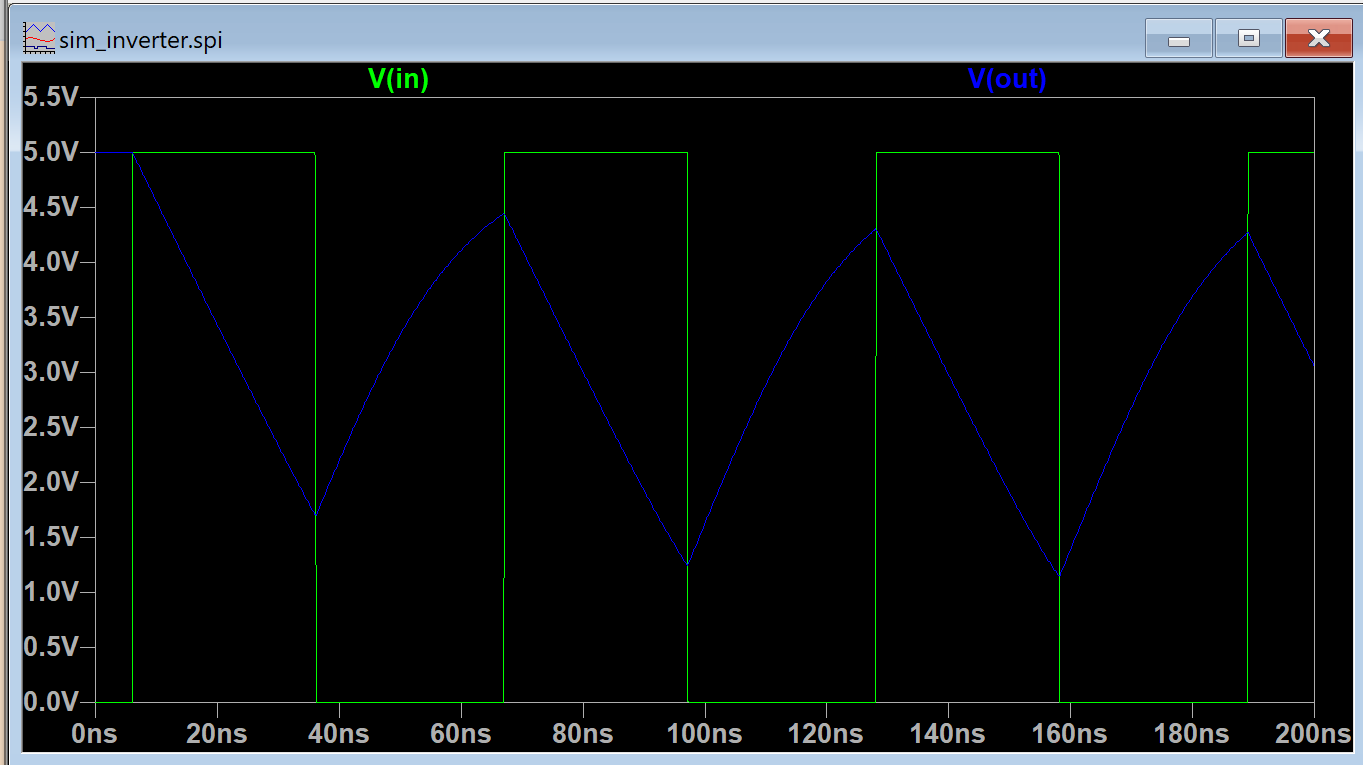
Figure 15. The input of the inverter and the output is graphed above.
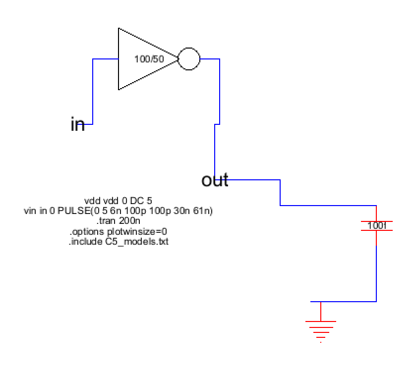
Figure 16. The 100/50 inverter is connected to a 100fF capacitor.
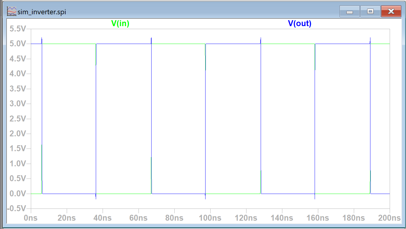
Figure 17. The input of the inverter and the output is graphed above.
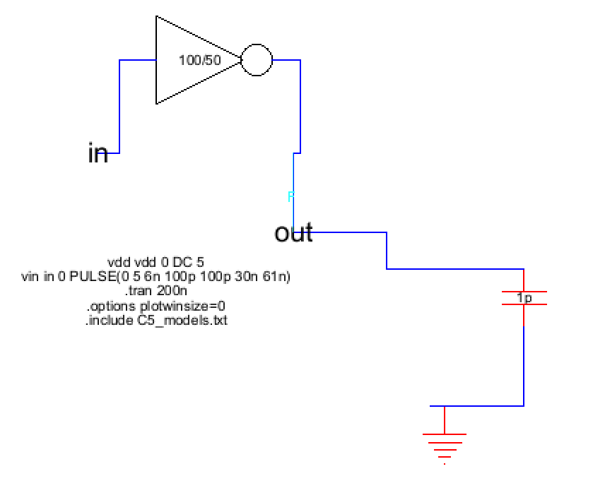
Figure 18. The 100/50 inverter is connected to a 1pF capacitor.
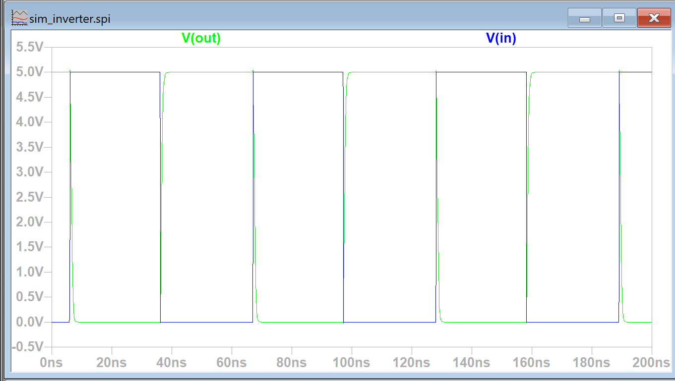
Figure 19. The input of the inverter and the output is graphed above.
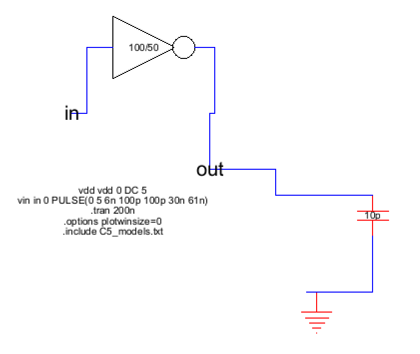
Figure 20. The 100/50 inverter is connected to a 10pF capacitor.
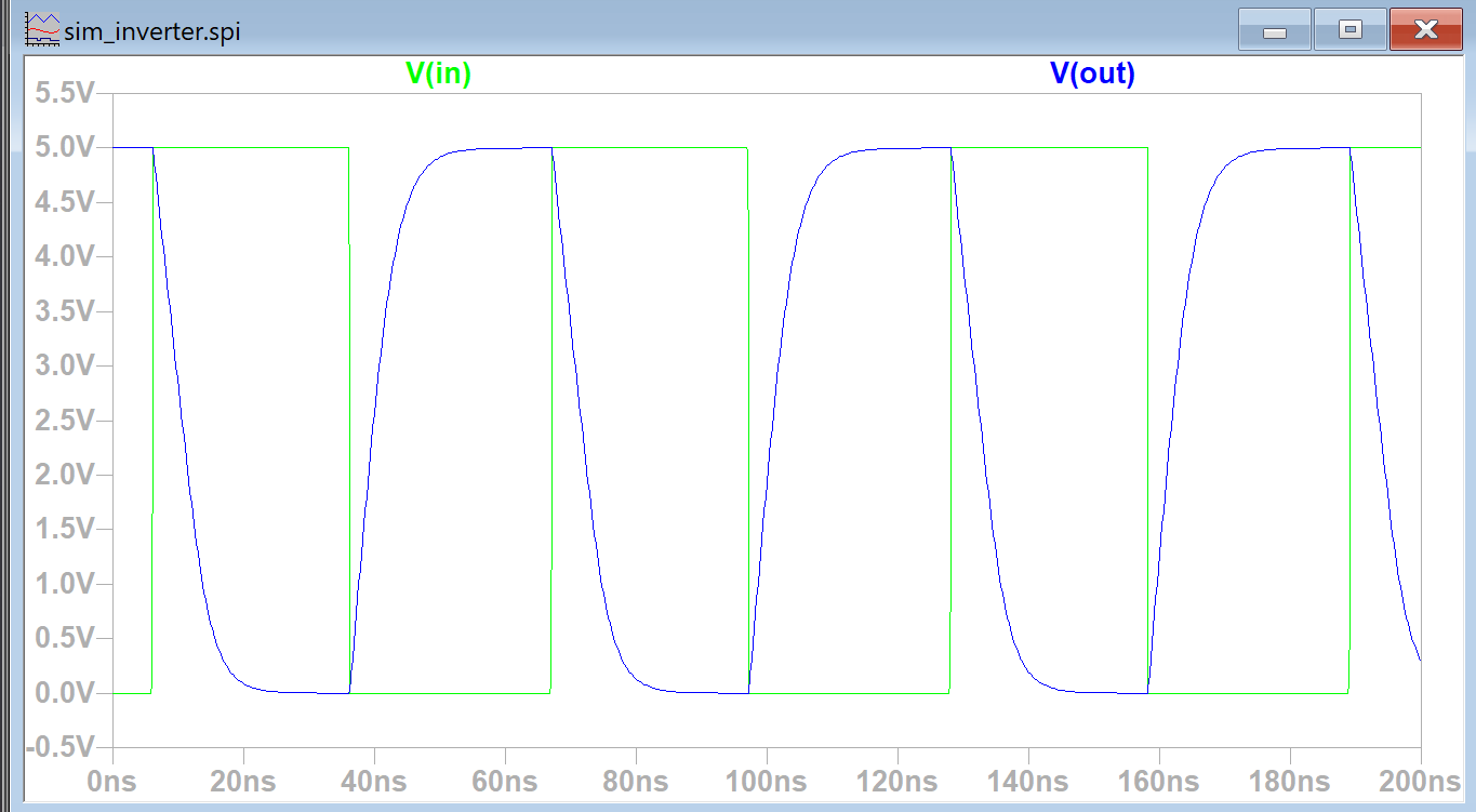
Figure 21. The input of the inverter and the output is graphed above.
Task 5:
In this task we used a different simulation tool that is built into Electric VLSI called ALS.
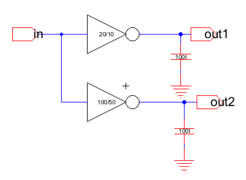
Figure 22. A schematic using both inverters driving 100fF capacitors was created.
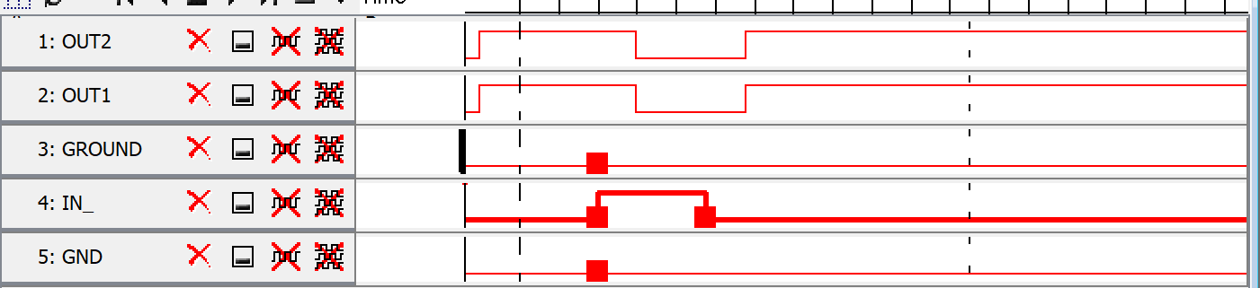
Figure 23. The output from the inverters was graphed in ALS alongside the input
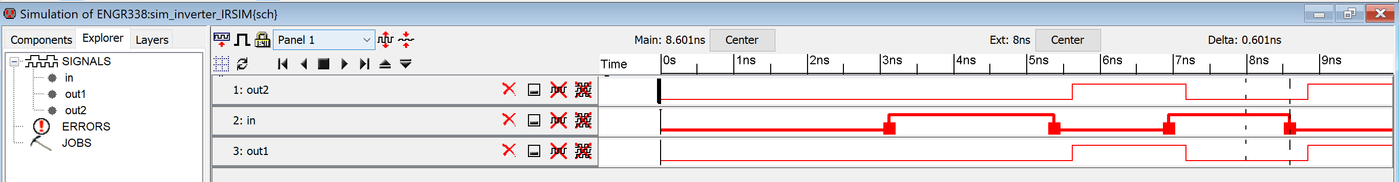
Figure 24. An alternate version of this simulation tool named IRSIM was also used.
In this task we created a schematic of the inverter using Electric VLSI
Figure 1. The schematic of the inverter is created using the PMOS and NMOS transistors.
Figure 2. Spice code is added to the iverter to ensure the input is inverted.
Figure 3. The output from LT Spice is plotted.
Figure 4. More LT Spice code is added to simulate a pulse wave input.
Figure 5. The output from LT Spice is plotted above.
Task 2:
In this task we created the layout of the inverter in Electric VLSI.
Figure 6. The layout of the inverter using both PMOS and NMOS transistors.
Figure 7. The inverter layout and schematic pass the NCC and DRC error checks.
Task 3:
In this task we used the multipler function in Electric VLSI to build a larger inverter. The previous inverter built was a 20/5-10/5 inverter while in this task we will create a 100/2-50/2 inverter.
Figure 8. The schematic of our previous inverter is duplicated and edited to accommodate for the larger size inverter.
Figure 9. PMOS and NMOS are connected in parallel to create a larger inverter.
Figure 9. The schematic and layout of the larger inverter passed both NCC and DRC error checks.
Task 4:
In this task we ran simulations in LT Spice to verify the driving capability of the two inverters. Both the inverters are connected to a 100fF, 1pF, and a 10pF capacitor and the output is graphed in LT Spice.
Figure 10. The 20/10 inverter is connected to a 100fF capacitor.
Figure 11. The input of the inverter and the output is graphed above.
Figure 12. The 20/10 inverter is connected to a 1pF capacitor.
Figure 13. The input of the inverter and the output is graphed above.
Figure 14. The 20/10 inverter is connected to a 10pF capacitor.
Figure 15. The input of the inverter and the output is graphed above.
Figure 16. The 100/50 inverter is connected to a 100fF capacitor.
Figure 17. The input of the inverter and the output is graphed above.
Figure 18. The 100/50 inverter is connected to a 1pF capacitor.
Figure 19. The input of the inverter and the output is graphed above.
Figure 20. The 100/50 inverter is connected to a 10pF capacitor.
Figure 21. The input of the inverter and the output is graphed above.
Task 5:
In this task we used a different simulation tool that is built into Electric VLSI called ALS.
Figure 22. A schematic using both inverters driving 100fF capacitors was created.
Figure 23. The output from the inverters was graphed in ALS alongside the input
Figure 24. An alternate version of this simulation tool named IRSIM was also used.