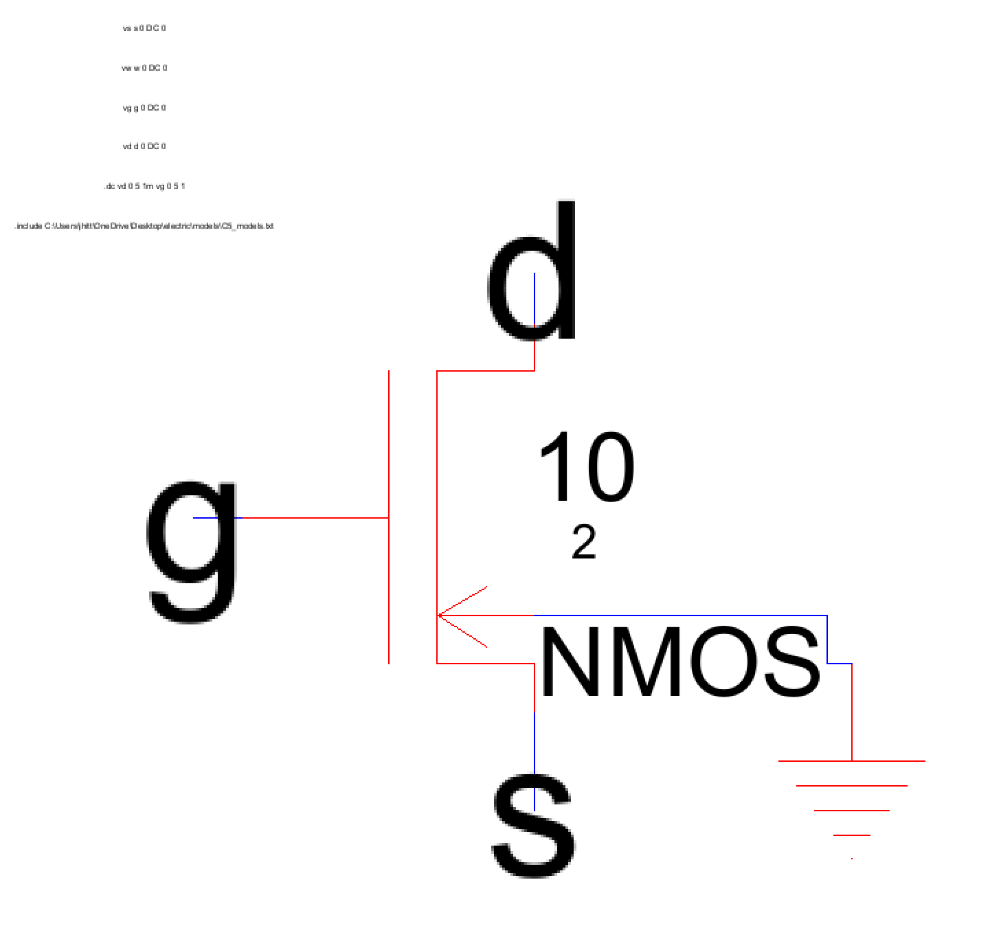
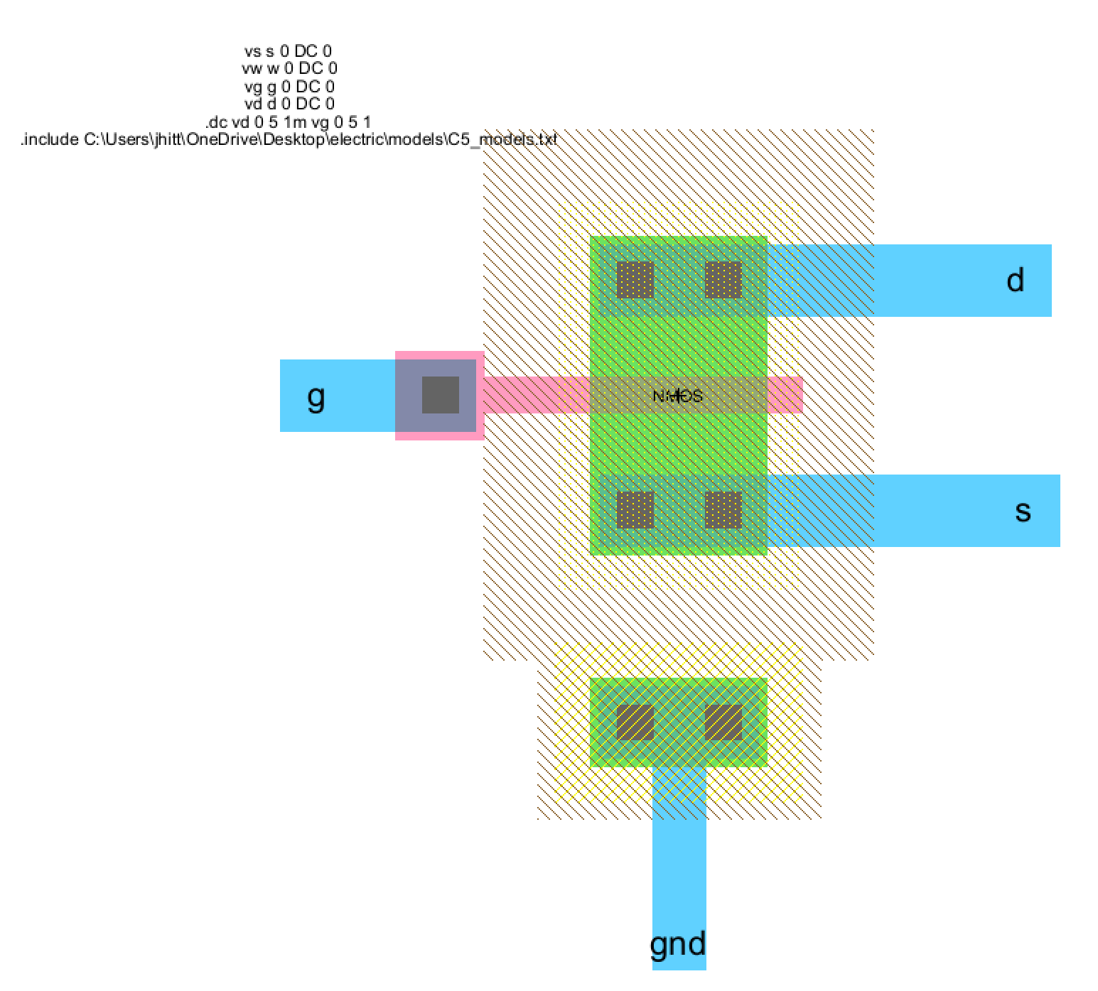
 Figure 2. The layout of the NMOS transistor.
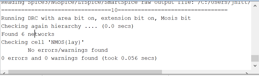
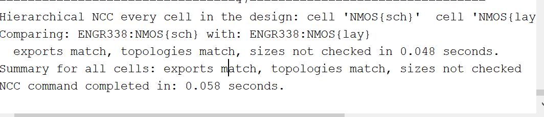
Once
these components were properly connected, they could then be checked
using both the DRC error checking method and the NCC error checking
method.
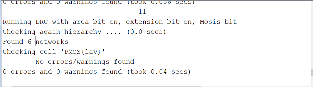
Figure 3. The NMOS transistor passed DRC error checks
Figure 4. The NMOS transistor passed NCC error checks
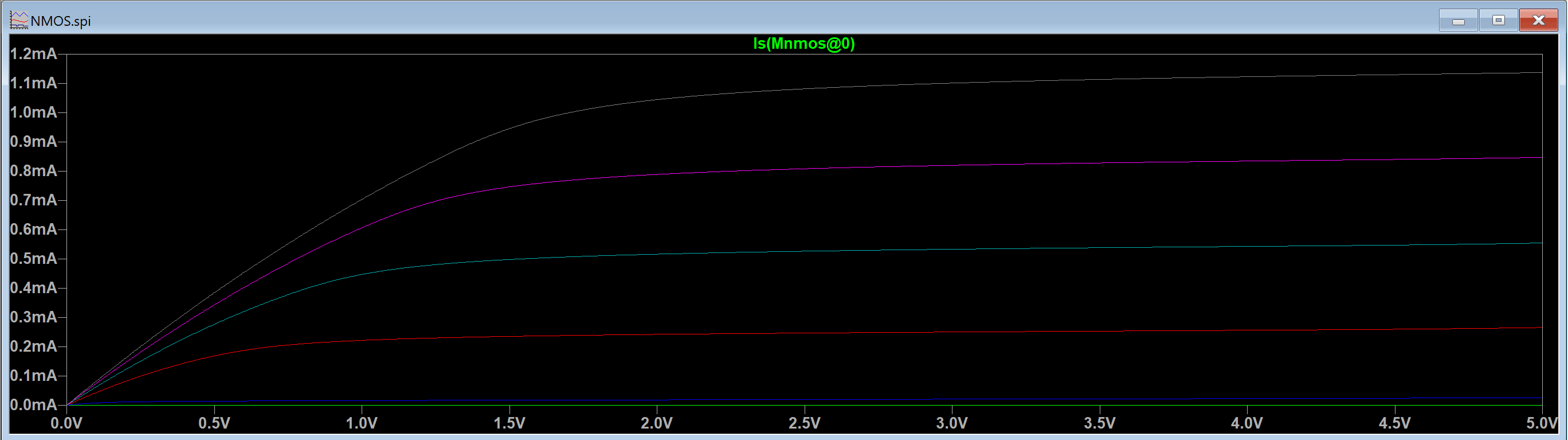
Once
the schematic and the layout had been verified an LT Spice script was
added and the simulation was ran on the transistor. Plotted below is
the source current of the NMOS device.
Figure 5. The simulation results from LT Spice for the NMOS transistor
This process was then repeated for the PMOS transistor.
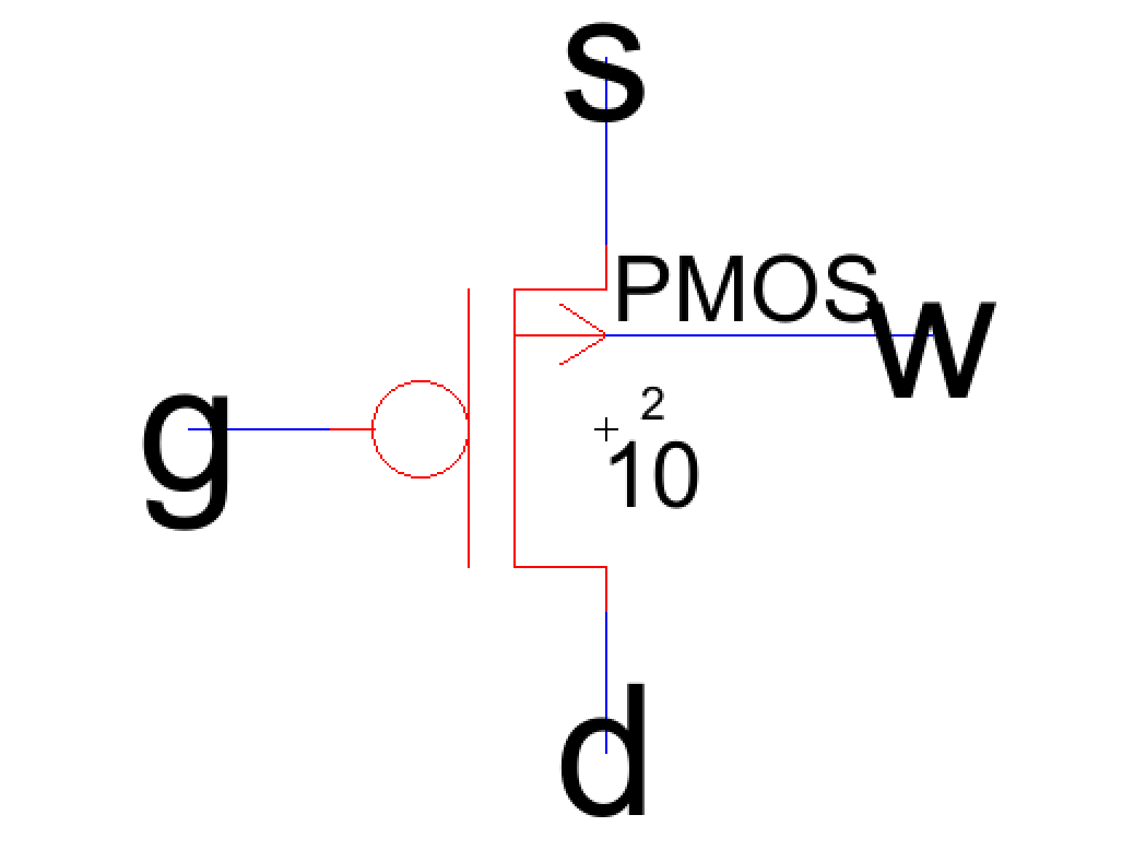 Figure 6. The Schematic of the PMOS transistor
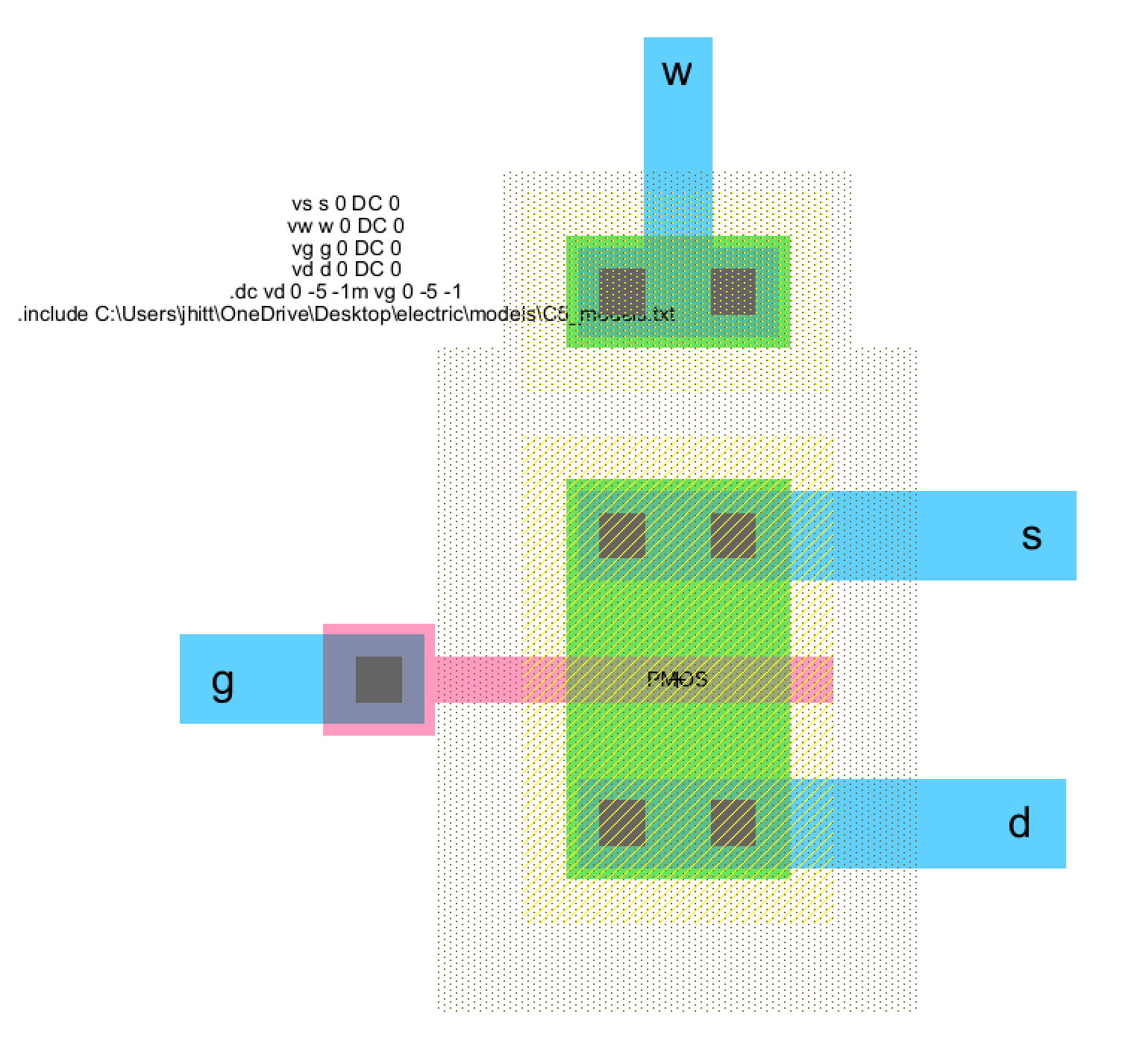 Figure 7. The layout of the PMOS transistor.
Figure 8. The PMOS transistor passed DRC error checks
Figure 7. The layout of the PMOS transistor.
Figure 8. The PMOS transistor passed DRC error checks
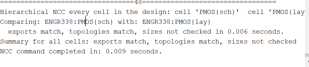
Figure 9. The PMOS transistor passed NCC error checks
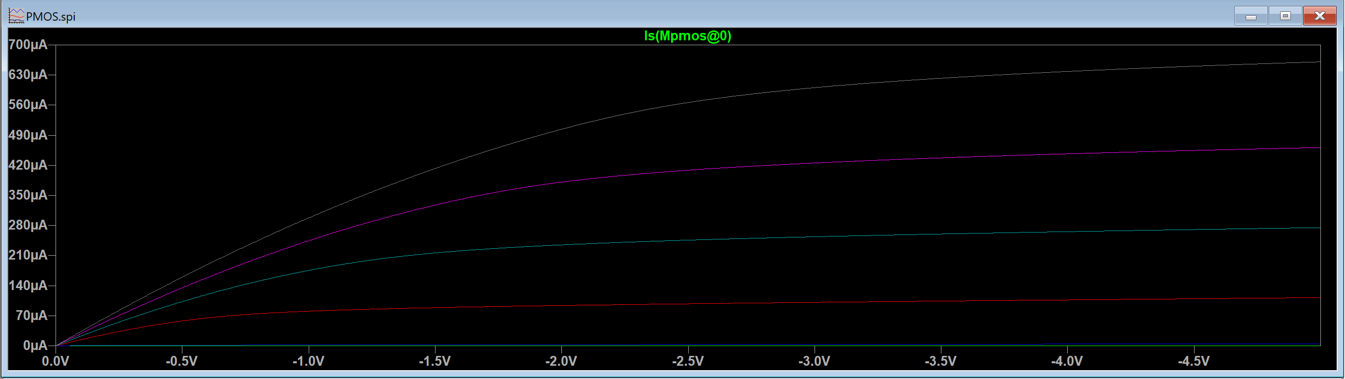
Figure 10. The simulation results from LT Spice for the PMOS transistor's source current
Discussion:
This lab was an excellent introduction to the internal design of
both PMOS and NMOS transistors. This lab helps to show how the internal
structure of these transistors is designed and how they operate. This
lab also helps to show the IV curves of these MOSFETS which further
describes their operation.