ENGR338 2020 Spring
Lab 3 - Layout the R-2R DAC
John Hitti

jdhitti@fortlewis.edu

Lab 3:
The purpose of this lab was to design a subcells and layout for the R-2R DAC in Electric VLSI using N-Well resistors in order to gain a better understanding of VLSI design using Electric VLSI and LTSpice.

Task 1:
In task 1 we used Electric VLSI to create subcells of the R-2R Ladder DAC. These subcells are an important aspect of VLSI design and are used to make components easier to build when schematics contain repeating components.

Figure 1. The repeating pattern in the R-2R ladder DAC is turned into a subcell


Figure 2. The subcell can then be implemented into the overall R-2R structure.


Task 2:
In task 2
we creates a layout of the subcells using n-well resistors in the C5 process. These resistors have a width of 15 and a length of 187.5 lambda. This is because the sheet resistance of the resistor is approximatly 800 ohms. Therefore, approximatly 12.5 squares are required to achieve the desired resistance of 10k ohm.

Figure 3. The layout of the subcell is created using n-well resistors.

Figure 4. The layout of the subcells can then be combine to construct the layout of the whole R-2R ladder.


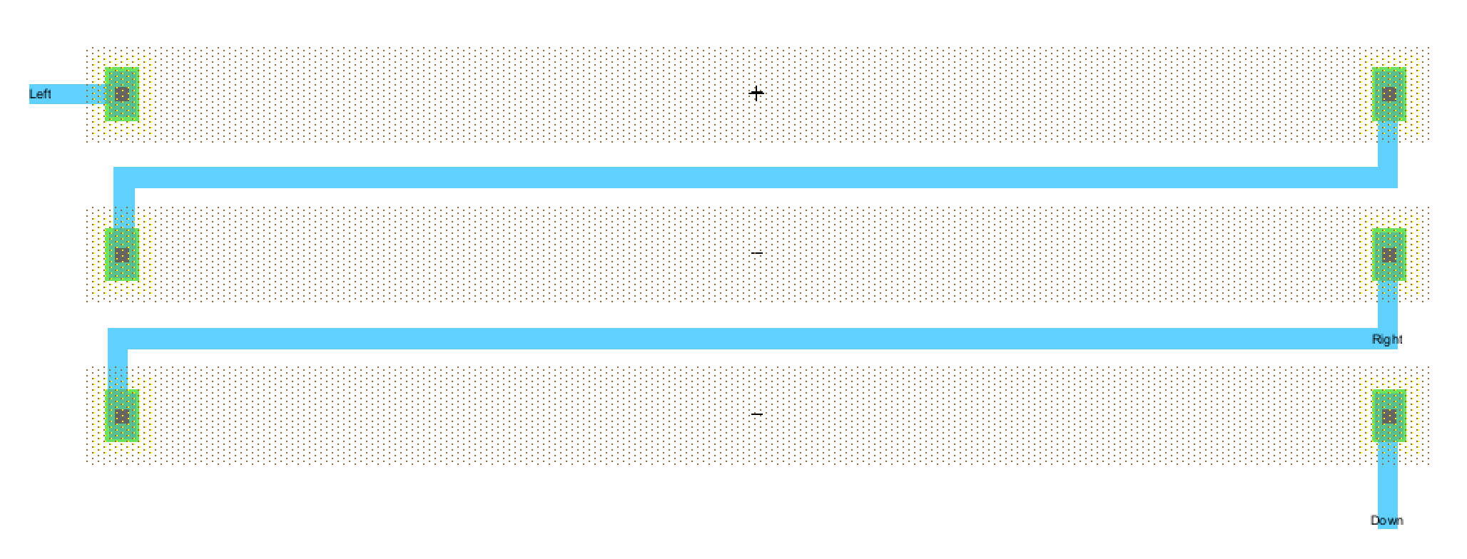
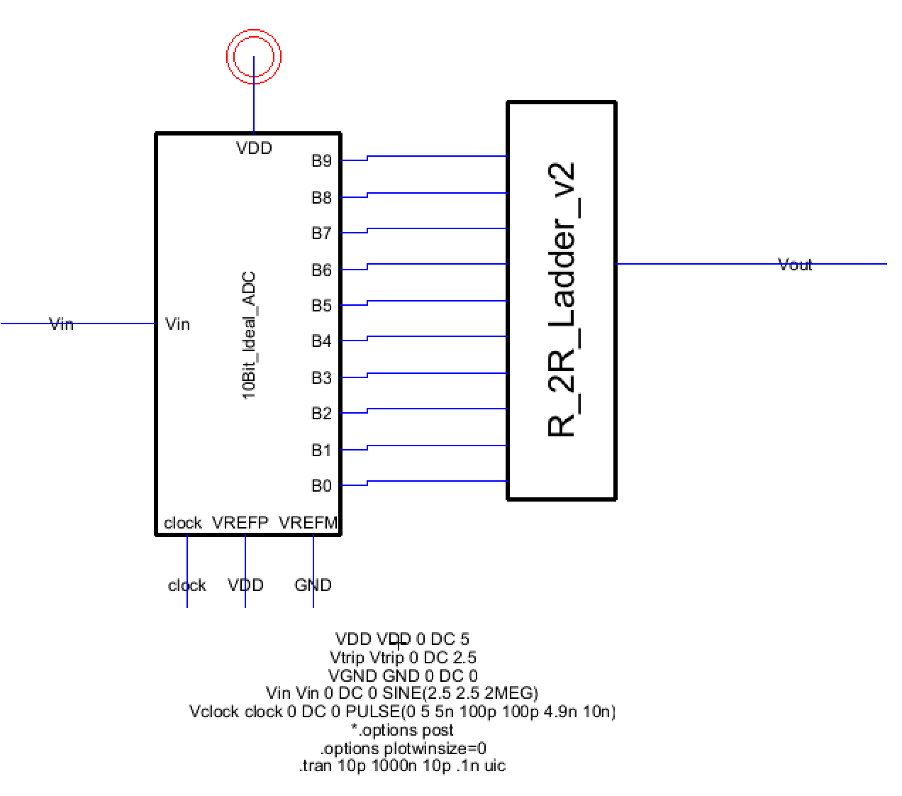
Figure 5. The R-2R DAC is then  connected to our ideal ADC for testing
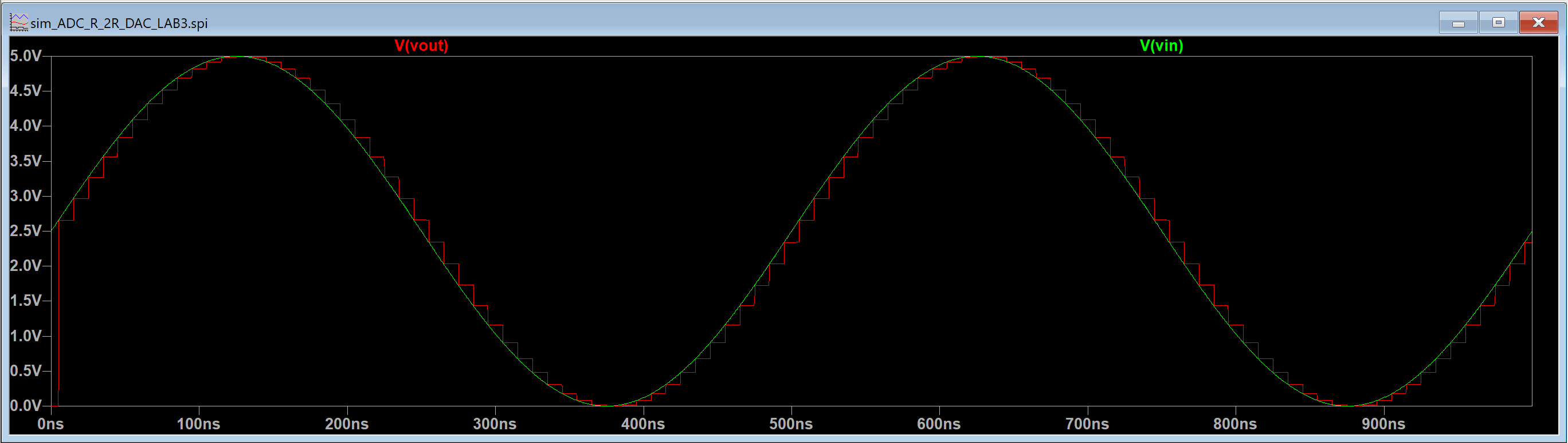

Figure 6. The output of the R-2R DAC is graphed alongside the input of the ADC showing the proper output


Discussion:
This lab was an excellent introduction to the use of subcells and layouts in VLSI design. This lab takes us one step further into understanding how common digital devices are designed and function. The use of subcells helps to greatly reduce the amount of work required to design a component with repeating patterns.