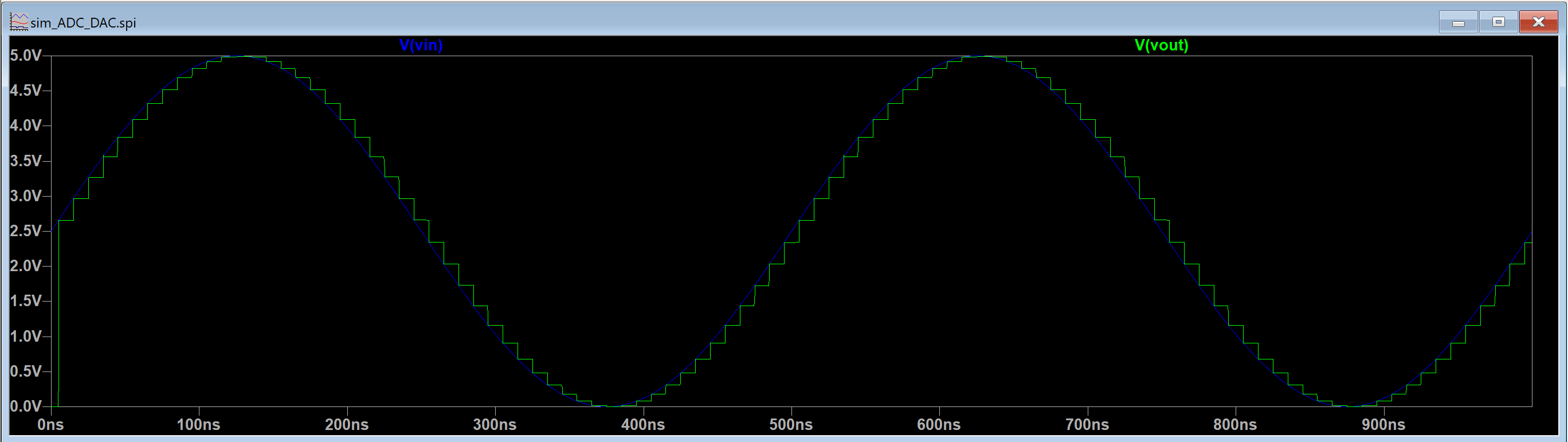
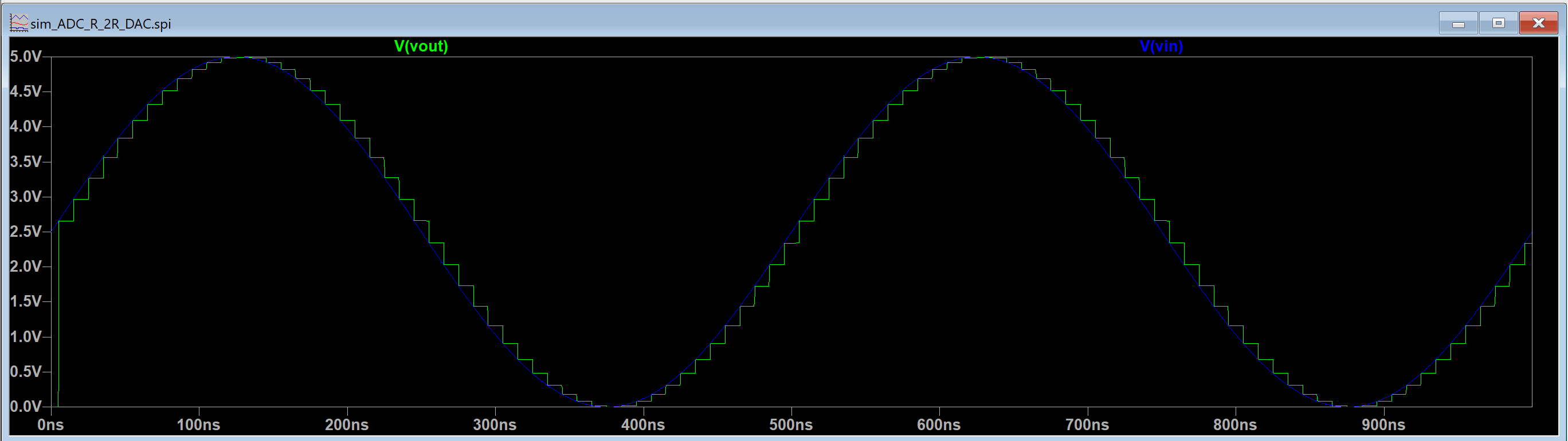
 Figure 5. The output of the R-2R DAC is graphed alongside the input of the ADC.
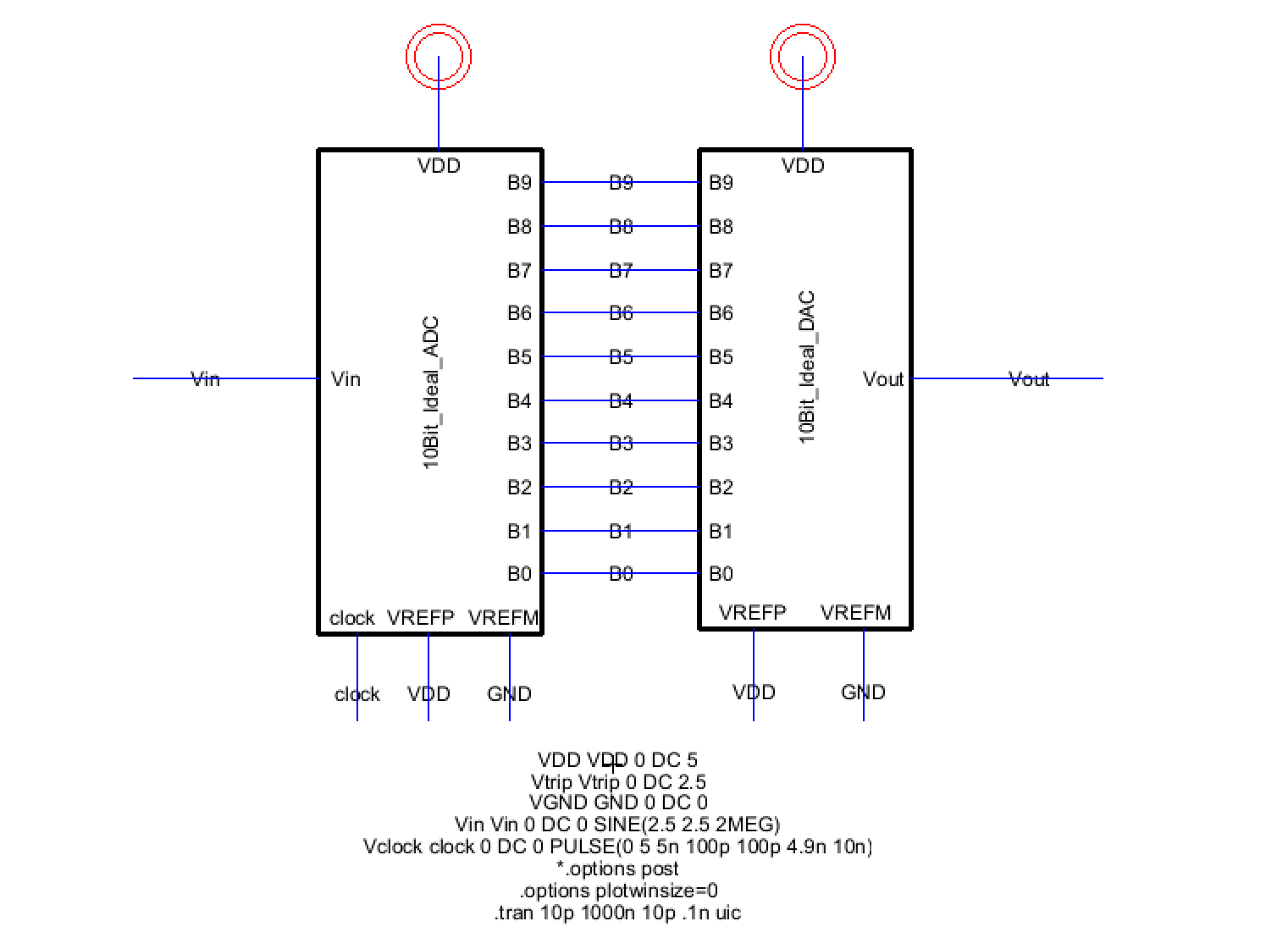
Task 3:
In task 3 we tested the time delay of the circuit when the
2-R2 DAC is driven only by the B9 pin and all others are shorted. The
load tested is a 10pF capacitor.
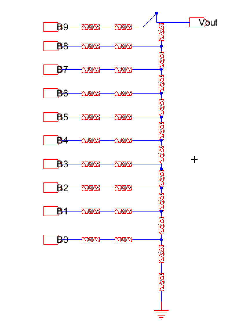
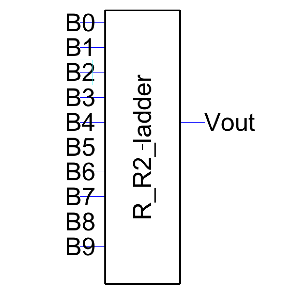
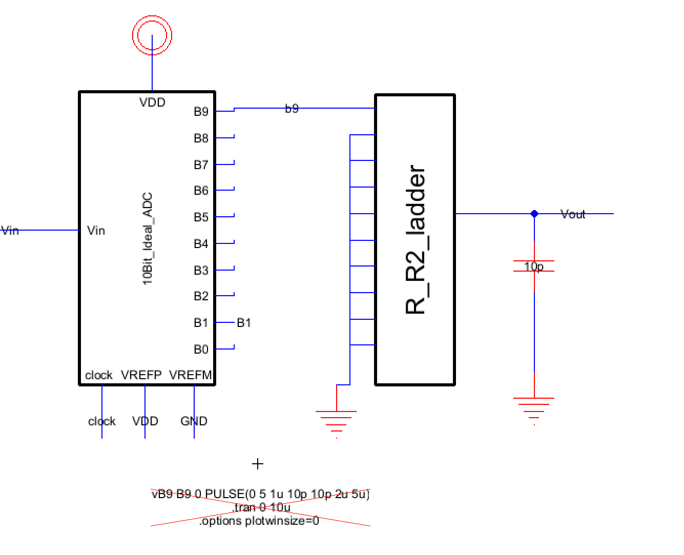 Figure 6. An
Electric VLSI schematic was made using the ideal ADC and R-2R DAC to
measure the time delay across the 10pF capacitor
Figure 6. An
Electric VLSI schematic was made using the ideal ADC and R-2R DAC to
measure the time delay across the 10pF capacitor.
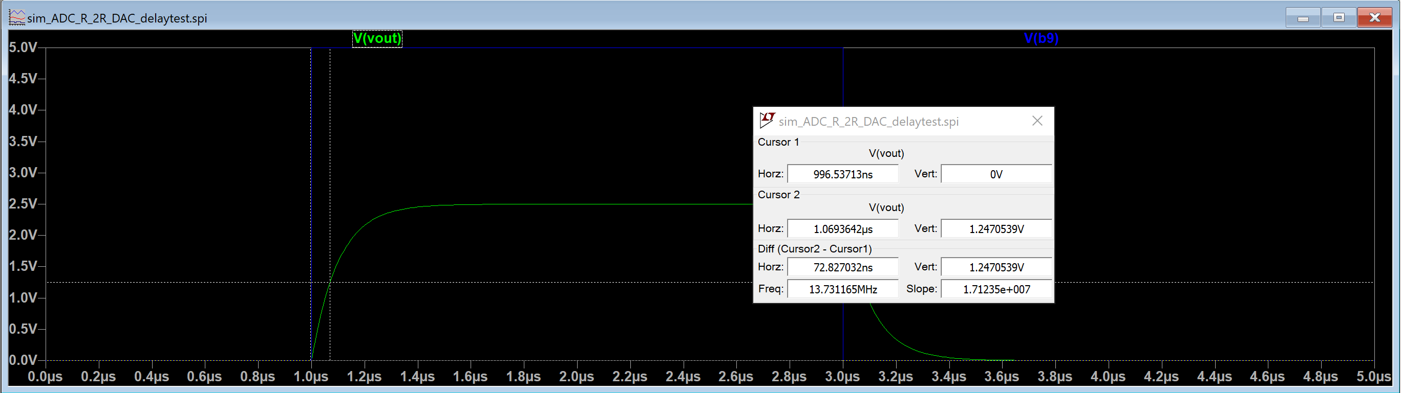
Figure 7. The output of the circuit was graphed and the time delay measured using LT Spice.
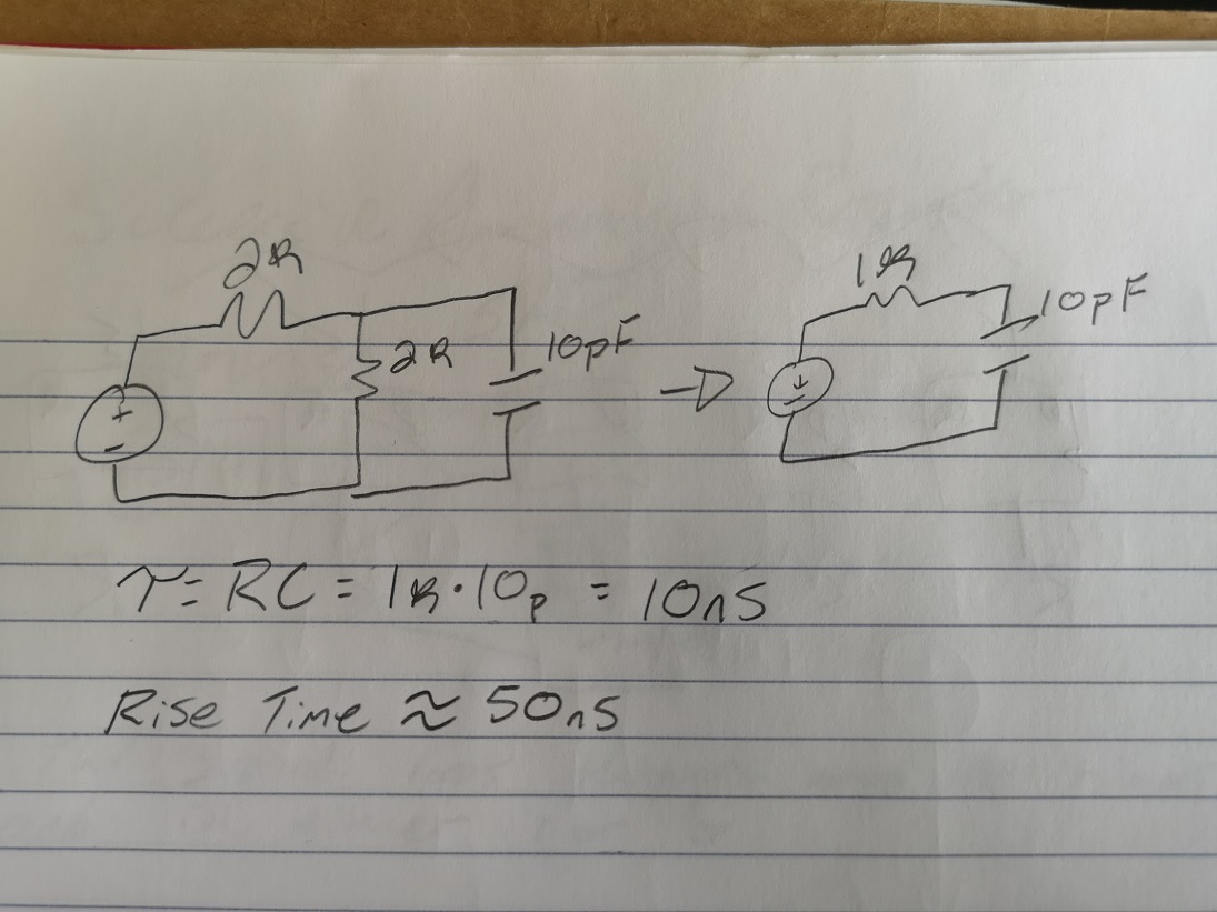
Figure 8. The time delay calculated in LT Spice is in line with the time delay calculated by hand.
Discussion:
This lab was an excellent introduction to the operations of both ADC and DAC components
and how they process digital and analog signals. Designing the 2-R2 DAC
helped to display the inner workings of this type of DAC and how it
converts digital signals to analog signals.