The
purpose of this lab was to create a power supply for future projects.
This power supply needed to be able to supply a current of a maximum of
3 amps at 5 and 3.3 volts DC with an input of 6-12 volts DC.
Materials and Methods
The power supply was designed using Eagle PCB and was the only software required to design the power supply circuit.
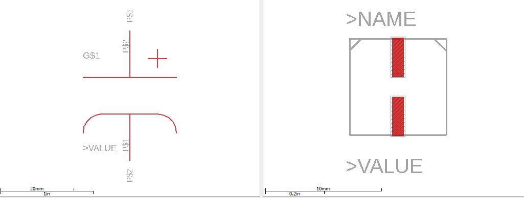
Custom schematics for devices needed to be created in order to properly design the circuit.
Figure 1. A custom polar capacitor in Eagle PCB
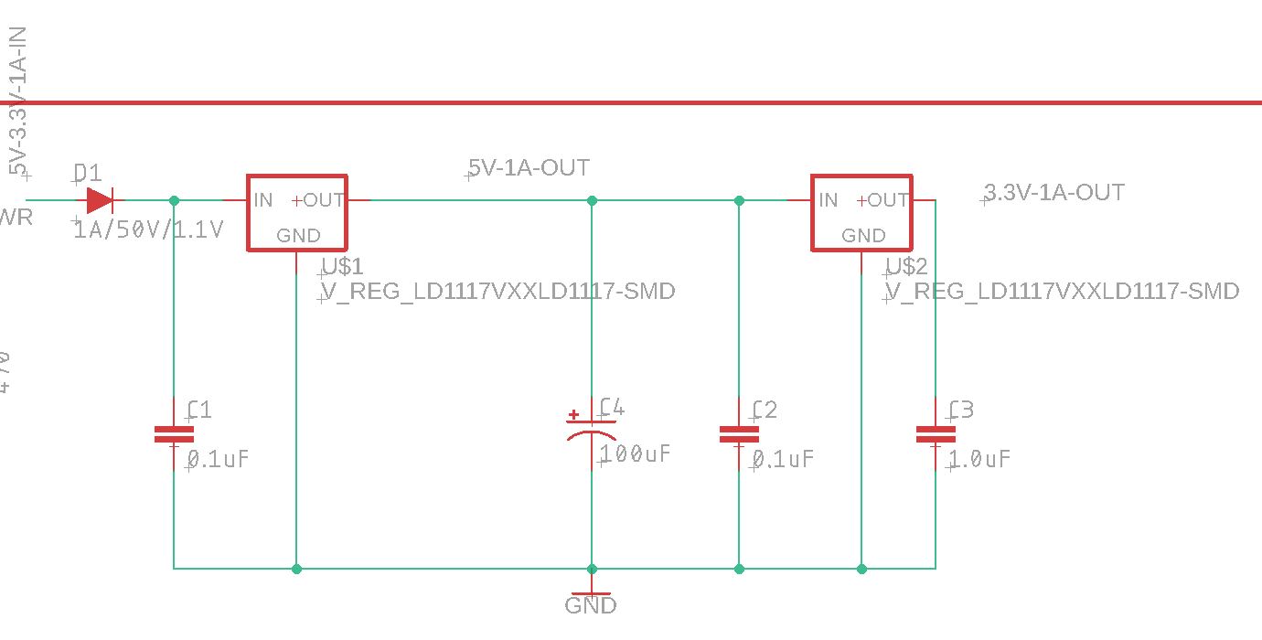
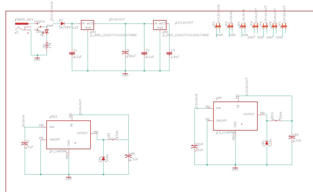
Using premade devices from the sparkfun library and custom devices we were able to create the following circuits. 5V/3.3V 1A DC Converter
This circuit can convert the input voltage to either 5V or 3.3V with a maximum of 1A of current.
Figure 2. 5V/3.3V at 1A DC Converter
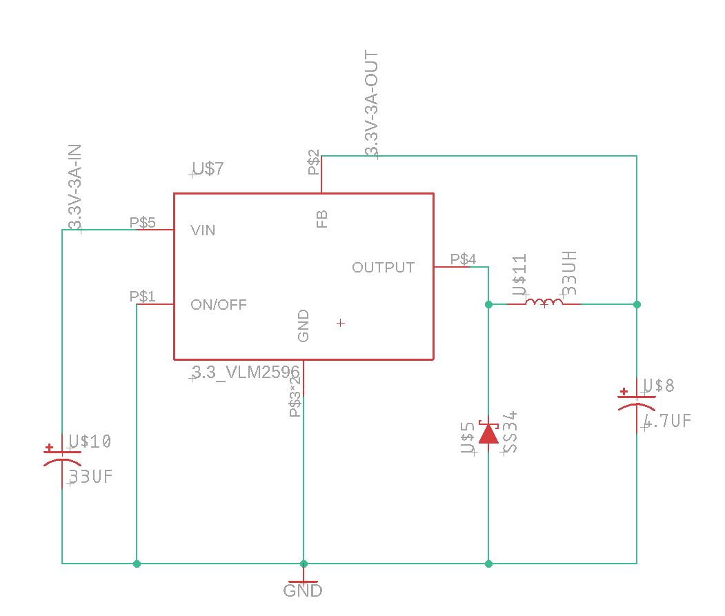
3.3V 3A Buck Converter
For devices that demand more current the following two buck converters are capable of delivering a maximum of 3A.
Figure 3. 3.3V at 3A Buck Converter
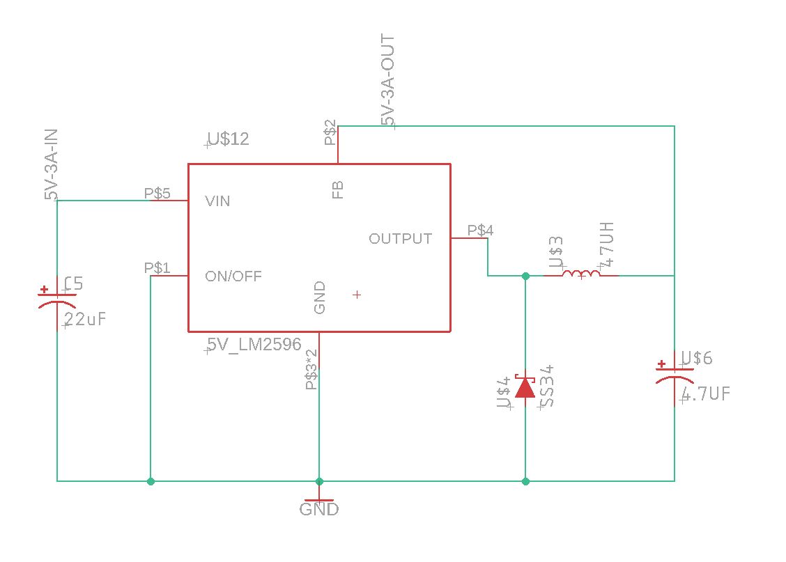
5V 3A Buck Converter
Figure 4. 5V 3A Buck Converter
Overall Schematic
Figure 5. Complete schematic of the power supply
Results
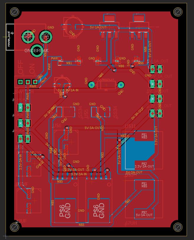
Once the circuits were connected the footprints of all
the devices were organized onto the Eagle schematic view to create a
design for physical pcb fabrication.
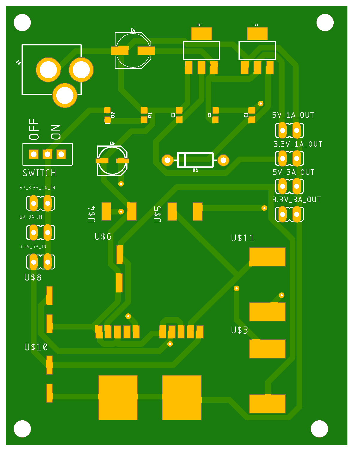
Figure 6. Finalized pcb design with copper traces in red and blue
Figure 6. Finalized pcb design using the manufacturing tab in eagle pcb
Discussion The error
checking software ran on this design reported no errors and therefore
it can be concluded that this device will be succeed in providing the
desired power and functioning correctly. This lab was a good
introduction to pcb design and helped to show how the process works. A
knowledge of pcb design will help to better understand how all the
parts on a board interact and ultimately how a microcontroller will interact with external devices.
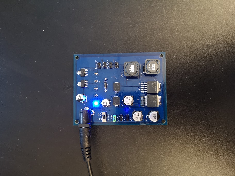
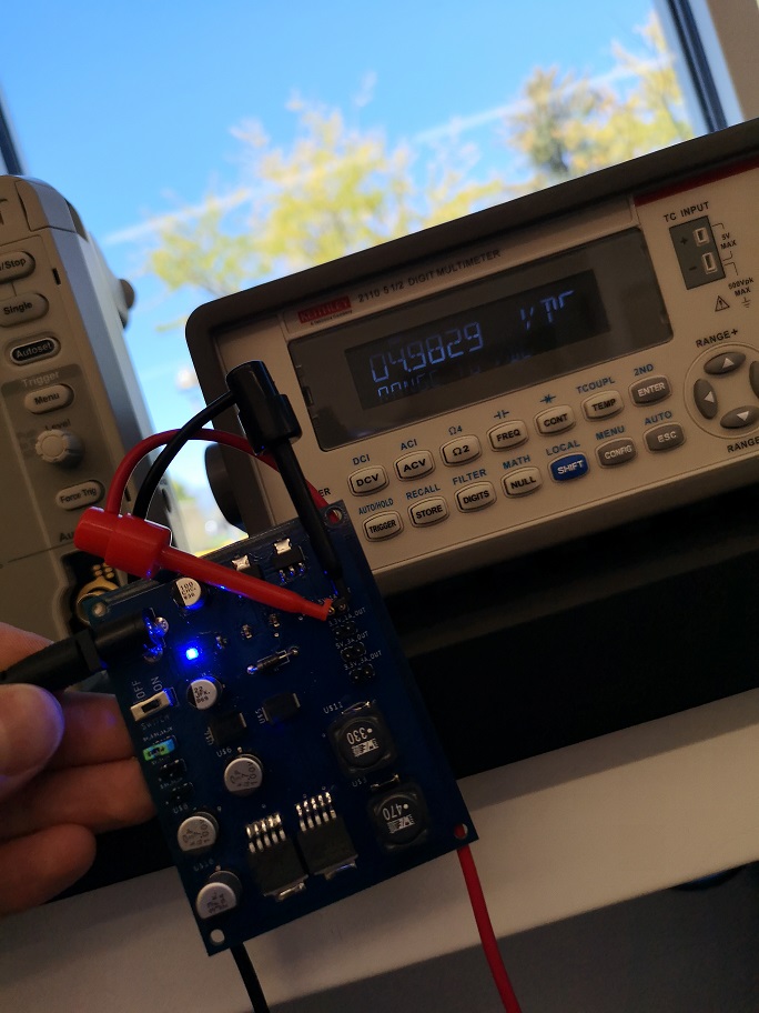
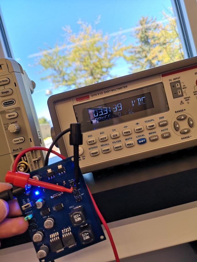
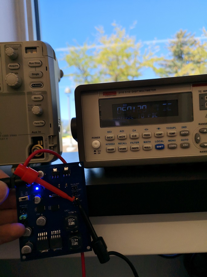
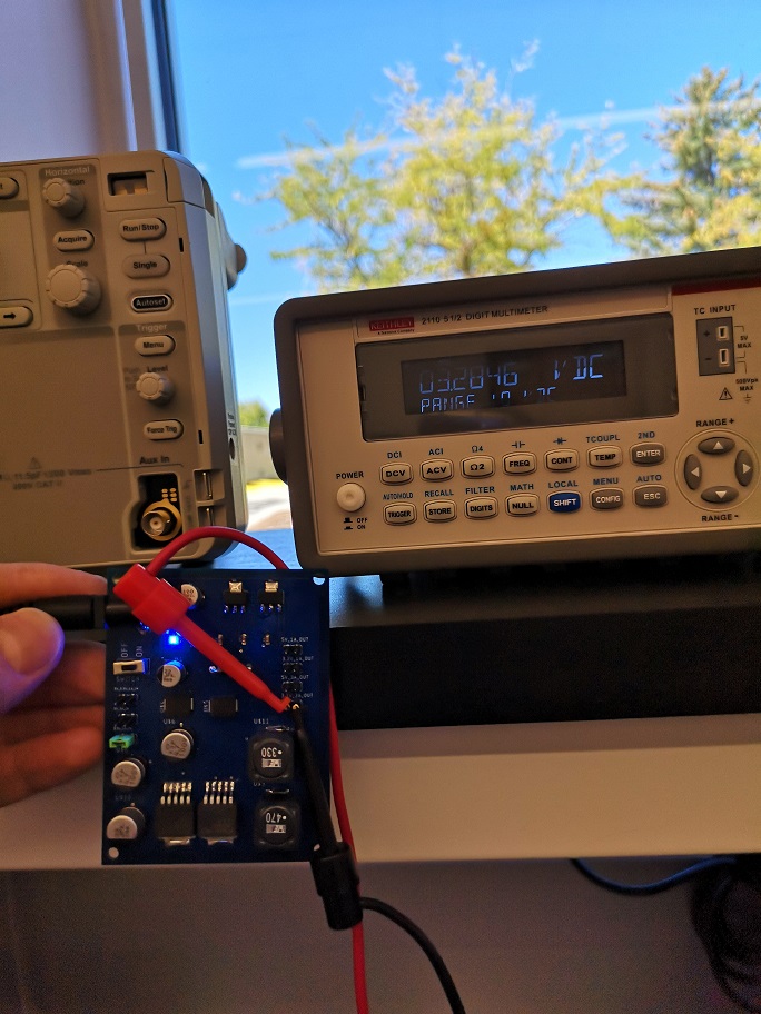
Finalized PCB Once
the device PCB arrived the components could be soldered onto the board.
This was done using a combination of the "hot air" technique using
solder paste, and the standard soldering iron method. All outputs where
then verified to function properly.
Figure 7. The final board with compontents solderd Figure 8. Verifying the 5 volt 1 amp output.