ENGR338 Lab 2021 Fall
Course Project
Name: David Lee
Email:
djlee1@fortlewis.edu
File of the completed Library: CE338ProjectDLee.jelib
Create
an 8-bit SAR ADC in Electric
Introduction:
In
this lab we used ElectricVLSI to build 8-bit SAR ADC, and LTSpice to
simulate it
Materials and Methods:
In this Lab we used the computer program ElectricVLSI to create the
schematics that were then simulated in LTSpice.
Results:
Task 1: Design the Sample and Hold Circuit
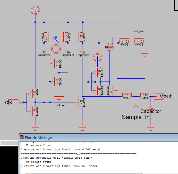
Figure 1: Shows the
Schematic of the Sample and Hold
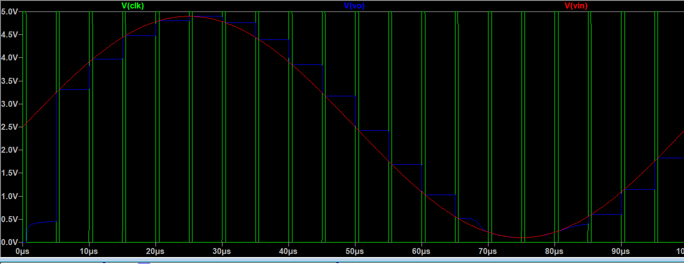
Figure
2: Shows the Simulation of the Sample and Hold
Task 2:
Operational Amplifier
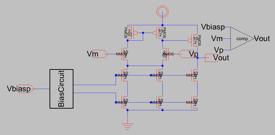
Figure 3: Shows the Schematic
of the Op Amp
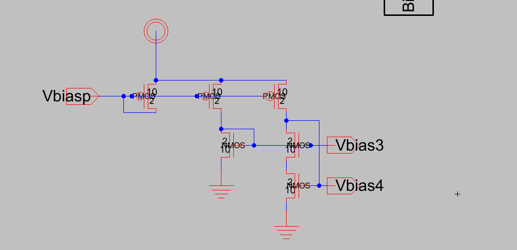
Figure 4: Shows the Schematic of the Bias
Circuit
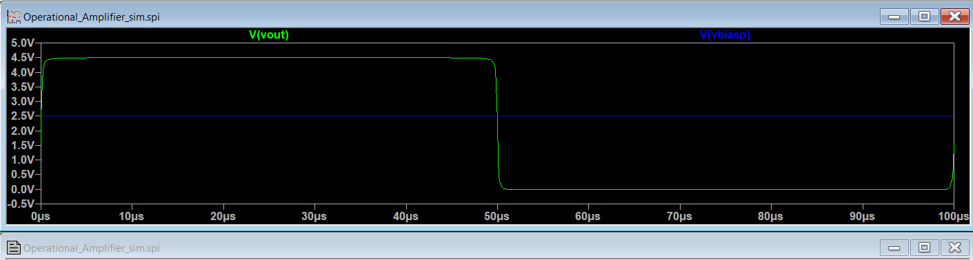
Figure 5: Shows the LTSpice
Simulation of the Op Amp
Task 3: Design
the SAR Block
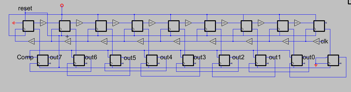
Figure
6: Shows the
SAR Block Schematic
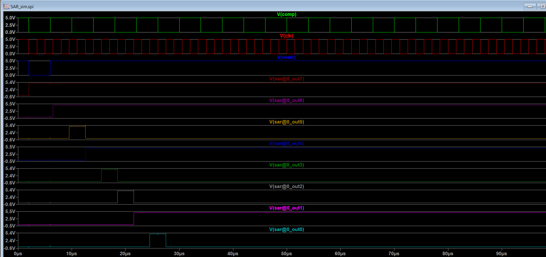
Figure 7: Shows the LTSpice Simulation of
the SAR
Task 4: Create an
R2R Ladder
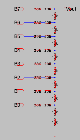
Figure 8: Shows the Schematic of the R2R
Ladder
Task 5: Create the
timing block and door Register
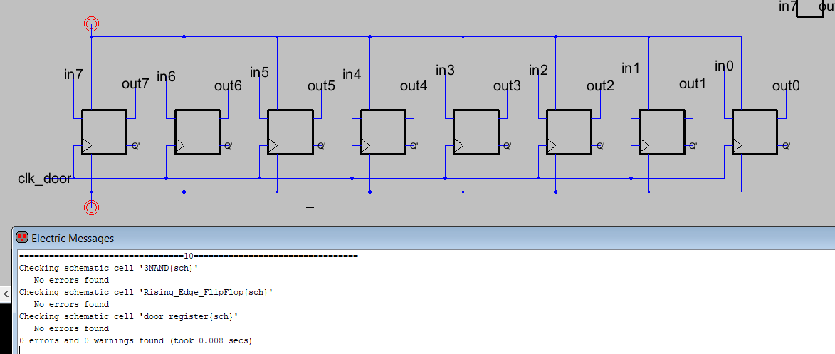
Figure 9: Shows the Schematic of the Door
Register
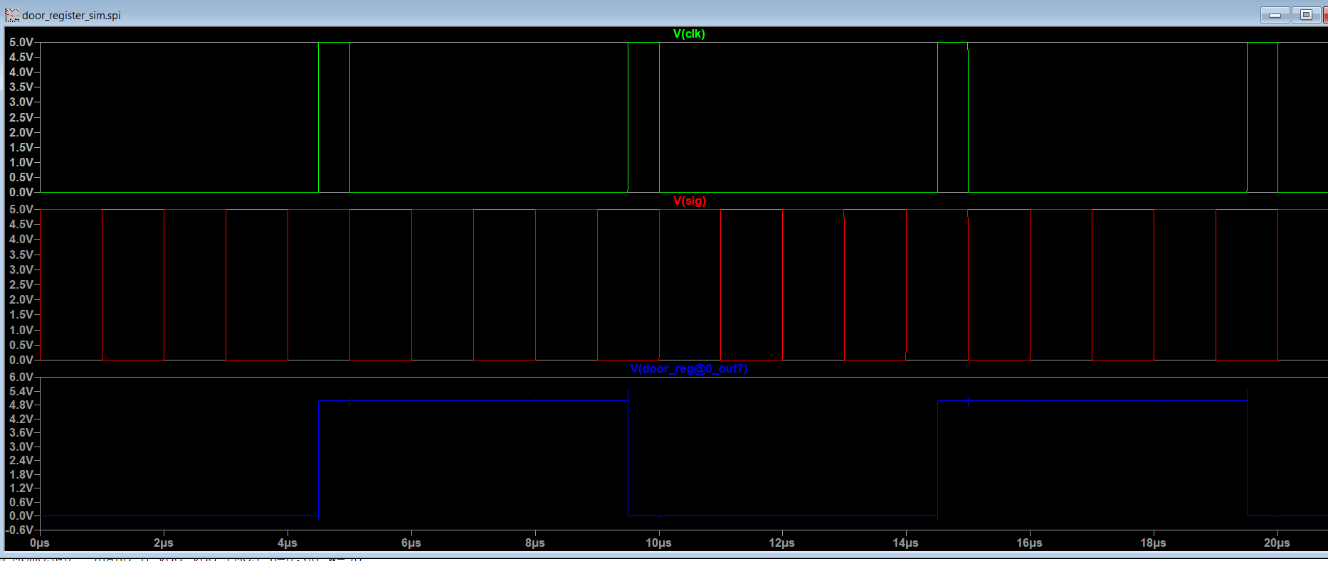
Figure 10: Shows the LTSpice Simulation of
the Door Register
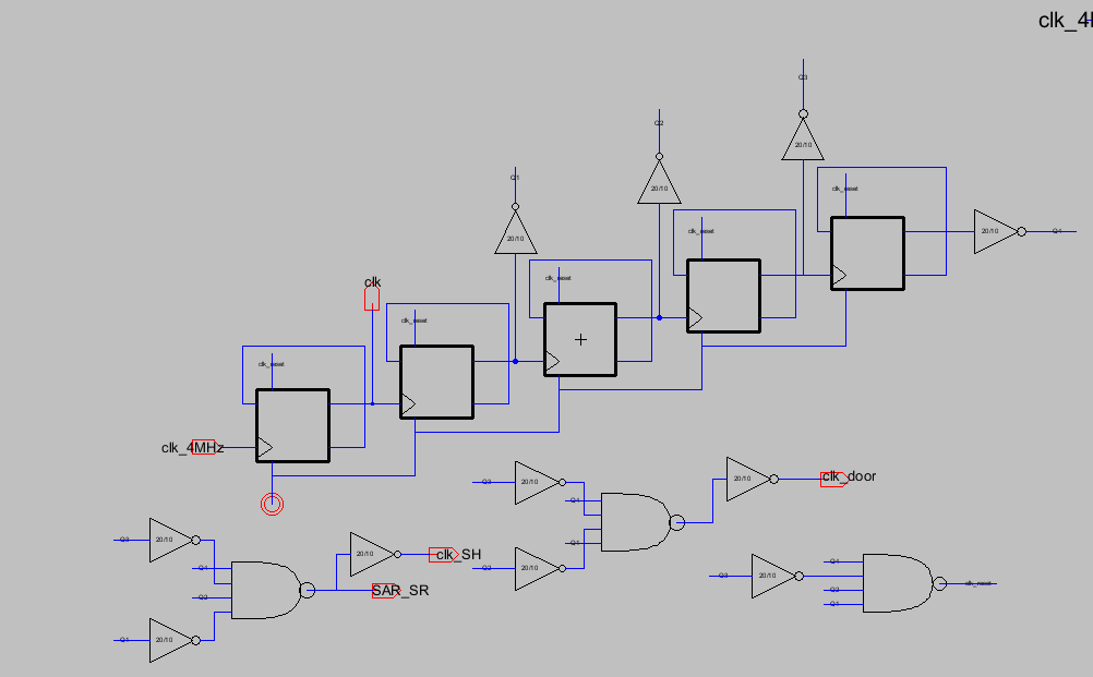
Figure 11: Shows the Schematic of the Timing
Block
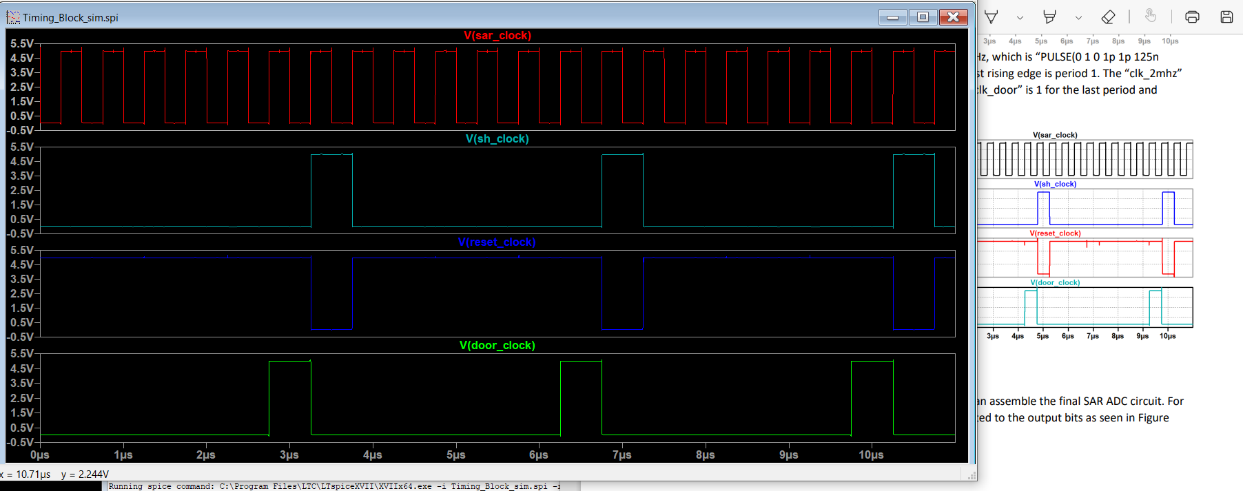
Figure 12: Shows the LTSpice Simulation of
the Timing Block
Task 6: Create the 8-bit
SAR ADC
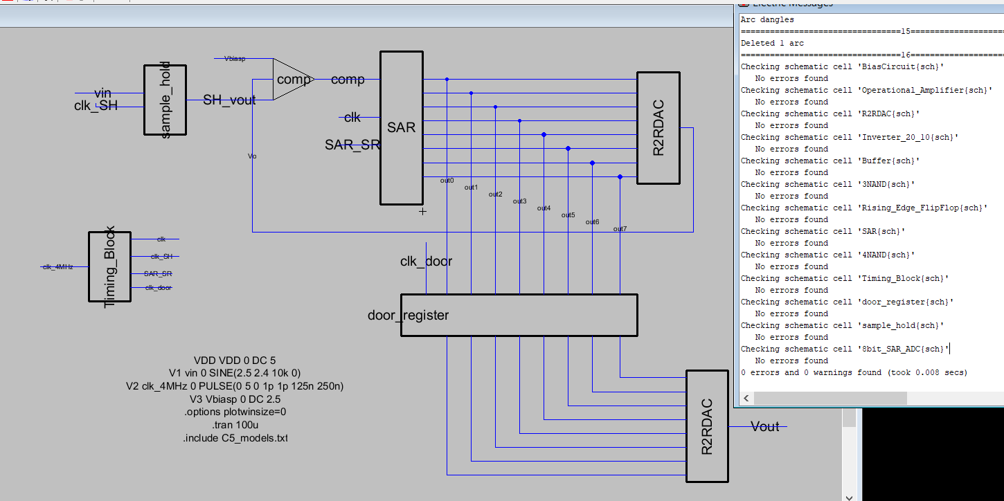
Figure 13: Shows the Schematic of the 8-Bit
SAR ADC and shows that all the componets have no errors when DRC is ran
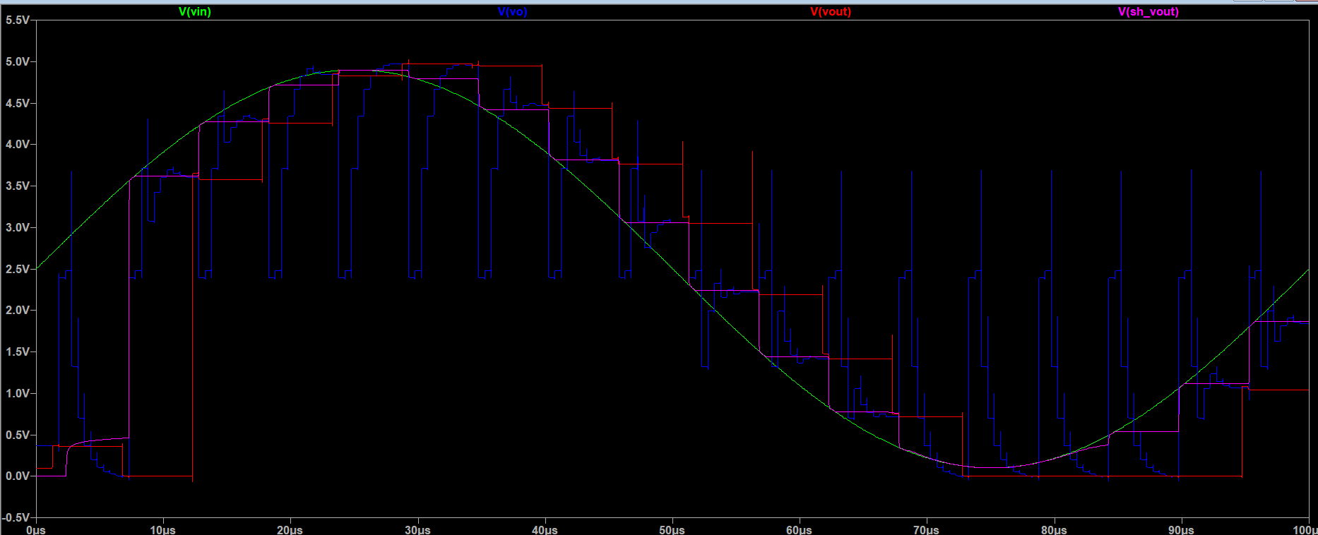
Figure 14: Shows the LTSpice Simulation of
the Completed 8-Bit SAR ADC
Task 7:
Answer Two Questions
Question 1: From
the example report drafted by Audra, there is a figure that shows the
vin/vout of the ADC. Dr. Li simulated a circuit and shows an
output. Why do they look so different? Does that mean Audra's ADC is
inferior to his?
Answer 1: The reason they look
so different is probably because the sampling rates were very
different. Although the simulations were ran for the same amount of
time, Dr.Li's Simulation had a faster sampling rate producing a
"cleaner"/more accurate result. And Audra's simulation probably
took a lot less time to run compared to Dr.Li's. This does not mean
that Audra's is inferior to Dr.Li's. This is because Audra could
probably be ran with the same spice code as Dr. Li's and produce the
same results.
Question 2: There is a huge
dip at the very beginning of the output. Does this mean that the ADC
fails converting the input into a digital signal so it is useless?
Answer 2: The huge dip at the very
beginning does not meant that the ADC is useless. This is just the
small amount of error that is produce because these converters are not
instant. They take a cycle or two inorder to get all the components
clocked and ready to go. This is just a small delay that will have to
be accounted for when putting this system into an application
Question 3: If you Probe the
output signal from the sample and hold circuit it looks exactly like
Vout. So why do we bother having all the other circuit blocks following
the S/H circuit for the conversion to get Vout? Why not just use
V(n002)?
Answer 3: The output signal that you
are getting is the correct shape of the output however it is still in
Analog form. It looks like it is in Digital because it not consistant
but that just because its grabbing small sections. The Reason we need
to keep the rest of the circuit blocks following the Sample and Hold
Circuit is because they are the components the do the conversion from
Analog to Digital.
Task 8:
What are the INL's and DNL's of this ADC
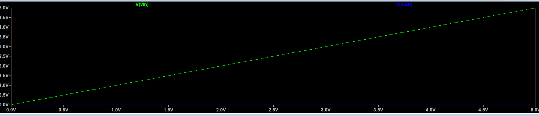
Figure 15: Shows the LTSpice Simulation of
the DC sweep Ran on the 8bit SAR ADC
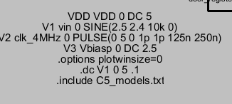
Figure 16: Shows the LTSpice code written to preform the DC sweep
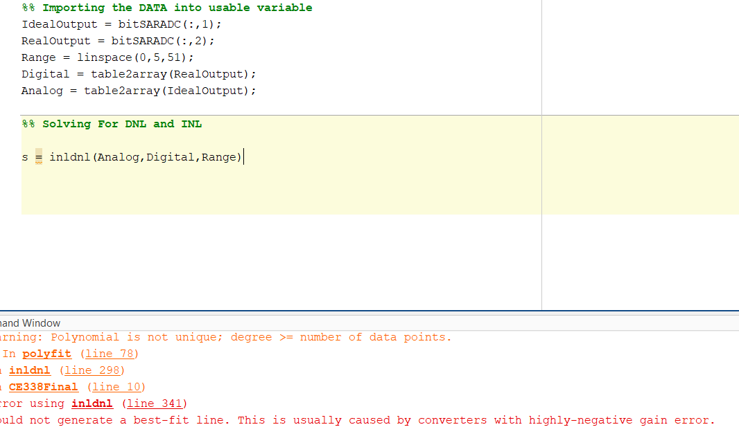
Figure 17: Shows the MATLAB code that would be used for calculating and plotting the INLs and DNLs
Discussion
This Project was able to be successfully completed to the standards
given because
the simulations of all the components are correct and all the componets
are DRC clean as we can see in Figure
12.
Even though each of the figures that hold the schematic show
that they are DRC clean the Final DRC ran on the entire Schematic shows
that all components are clean. This project was really fun to do
because it shows all the complex parts of Electric that are able to be
used. It showed me that you can pretty easily covert LTSpice circuits
and components into Electric Schematics. It takes a lot of time but it
is very do able. The problems that I faced during this lab was trying
to use the Operational Amplifier from the Project layout but I learned
that it was only able to do 0 to 1 volts no matter what. To solve this
issue I used an Operational Amplifier that I had previously created in
another Lab. This fixed the issue I was having with my Op amp not
functioning correctly. I used a couple of components from other labs
that either had do have minor modifications done to them or nothing.
These included the inverter, R2R ladder and a couple different gates. I
really enjoyed this project because I had to fully understand what the
circuit was doing and what it was suppose to be doing. I had to use my
brain inorder to solve issues that I was facing and how to change my
circuit to provide the expected results. Another problem I had
struggled with is getting the ciruit to work while preforming a DC
sweep so I would be able to calculate the INLs and DNLs. As you can see
from Figure 15 my input was correct but the output was way off.
You can also see that my MATLAB code was working for the calculations
but since the output is zero it creates too much error and the program
wont calculate it. But to Export the data was really simple. All you
have to do is run the simulation in LTSpice then select export data. It
will then Export the data as a .txt file which then is easily imported
and manipulated in MATLAB to get variables that are wanted.