CE338 Digital VLSI Design
Class Project - 8-bit SAR ADC


Connor O'Keefe
Email: cwokeefe@fortlewis.edu

Introduction:
This project goal is to build an 8-bit SAR analog to digital converter (ADC) using C5 technology. This requires the building of the following circuits:

Materials and Methods
Procedure
Building the SAR Block is shown below. The SAR block is made of multiple DFF registers and buffers.

Here is the
TI DFF with set and reset schematic/symbol.


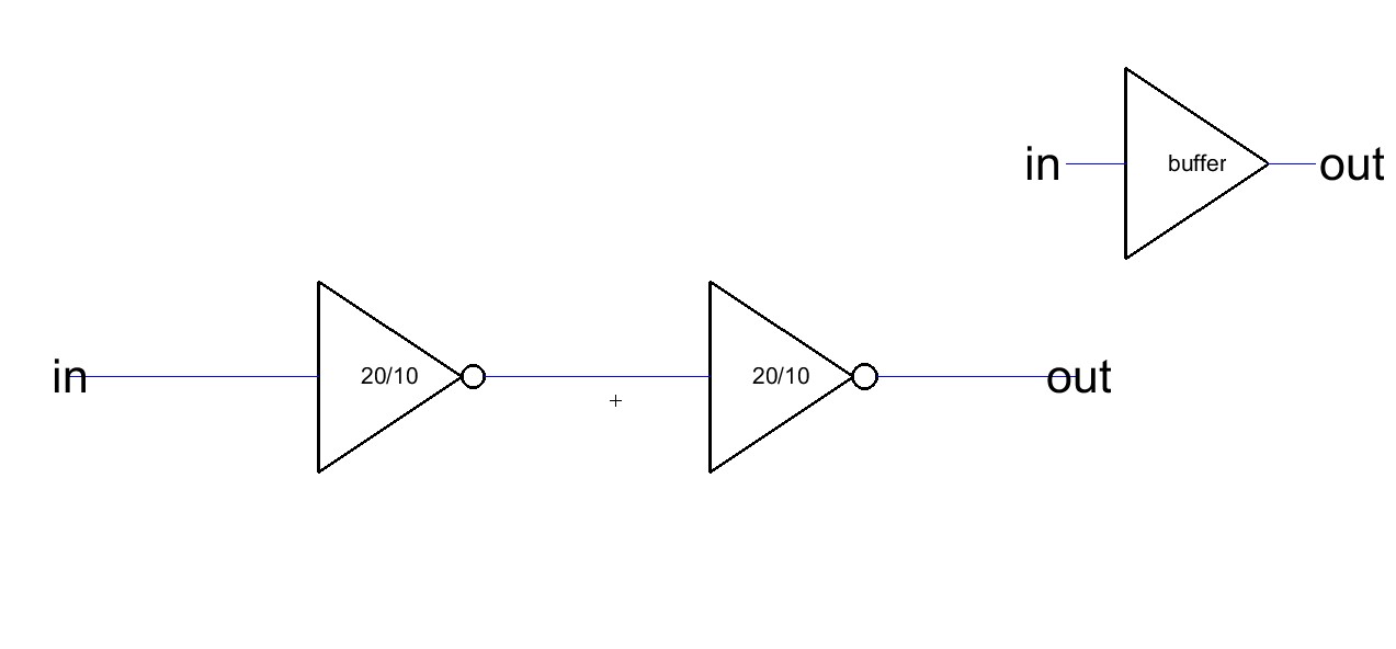
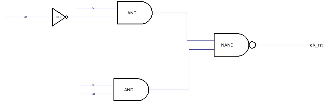
Here is the buffer schematic/symbol:


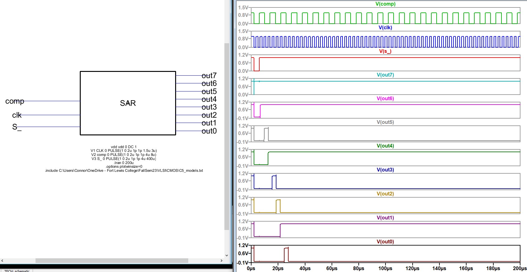
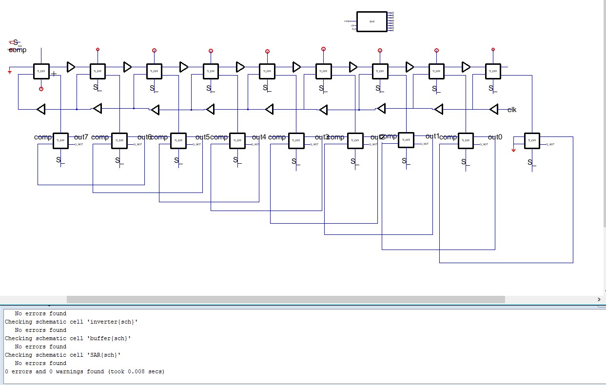
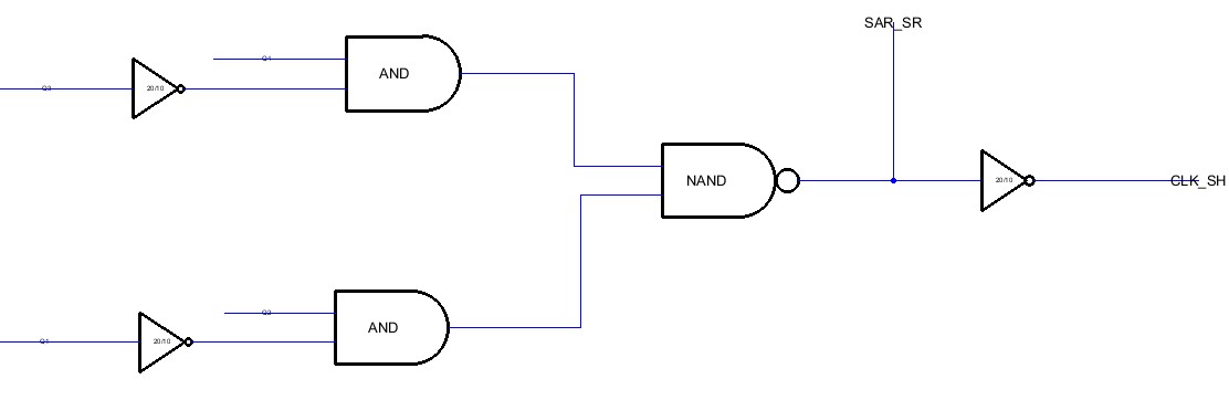
Here is the SAR schematic/symbol:


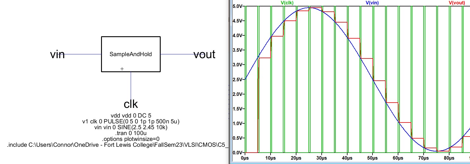
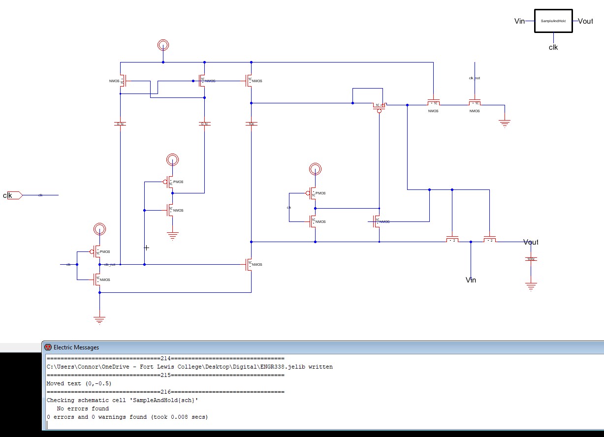
Here is the Sample and Hold schematic/symbol:


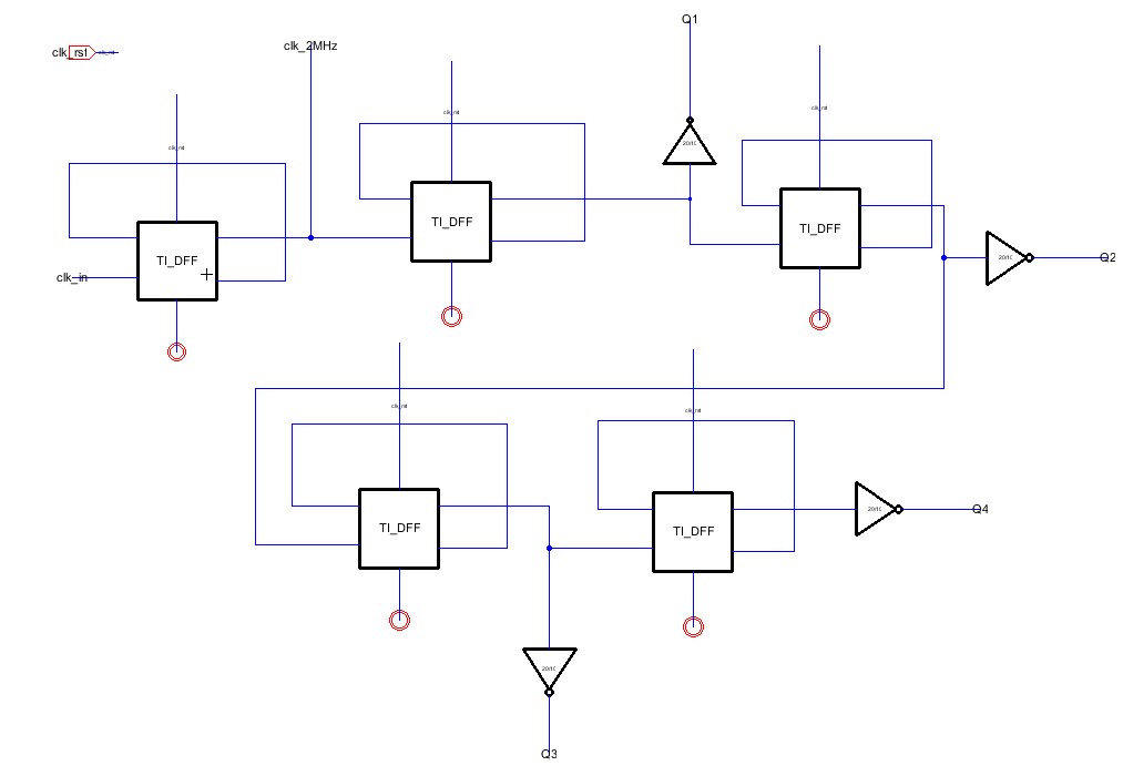
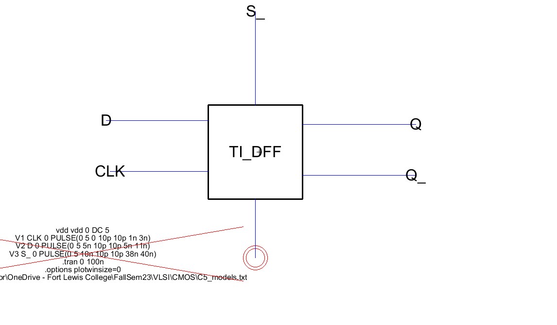
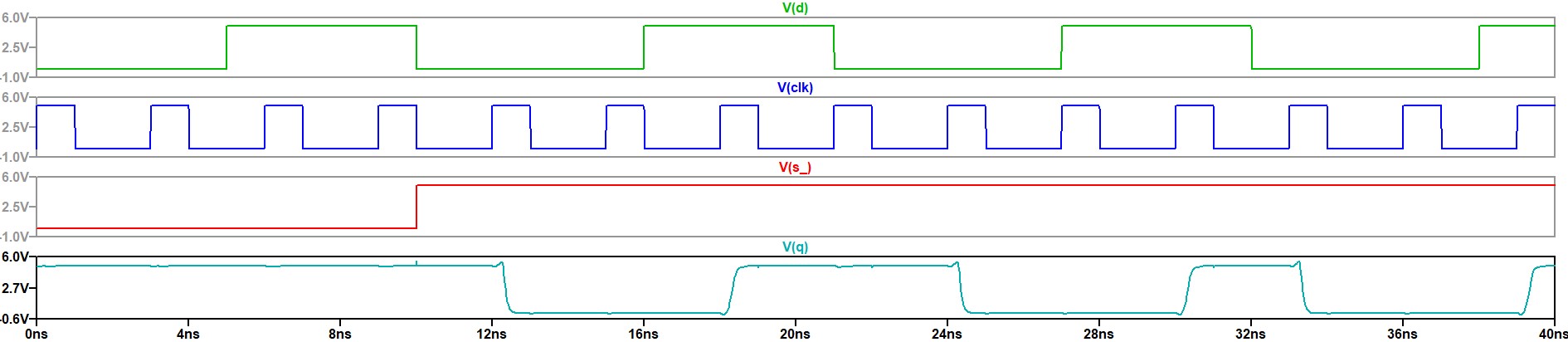
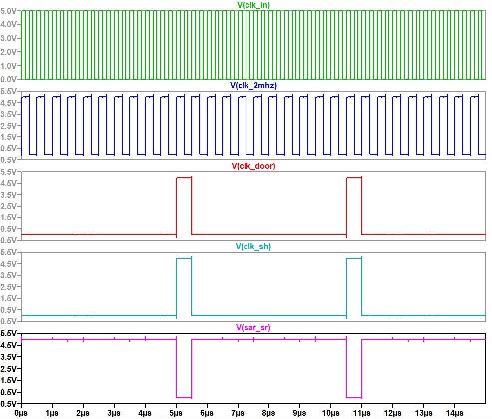
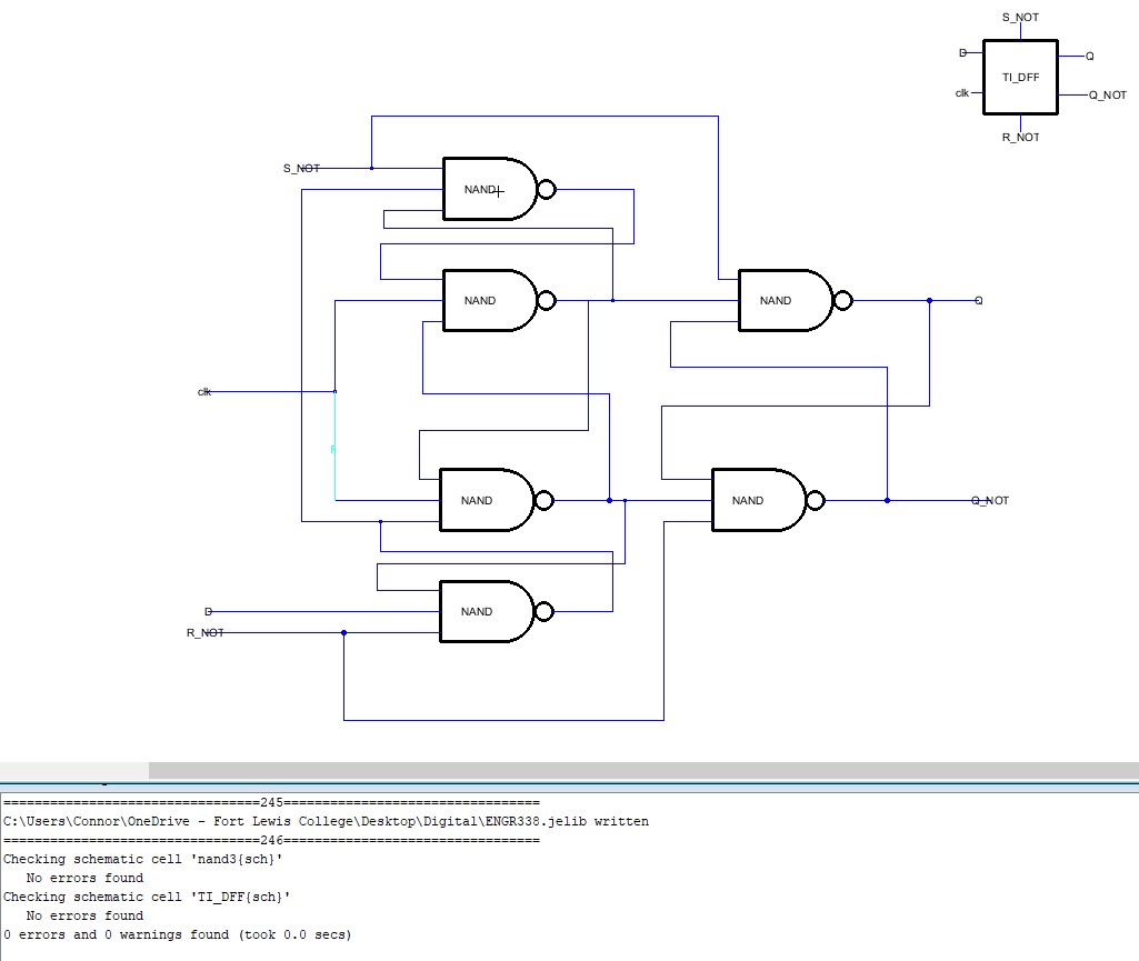
Here is the schematic for the Clock Register:


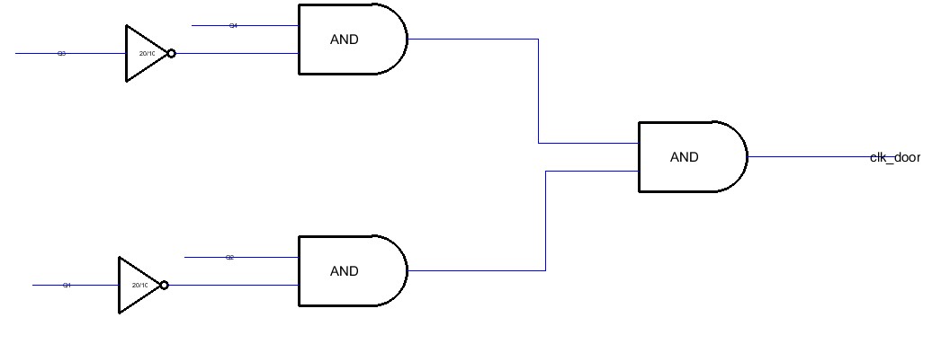
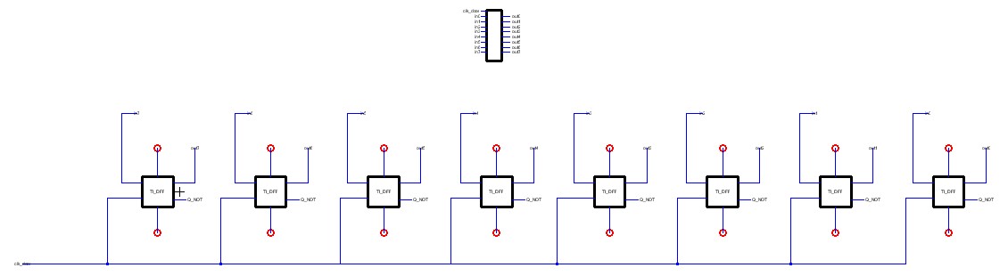
Here is the Door Register Schematic:


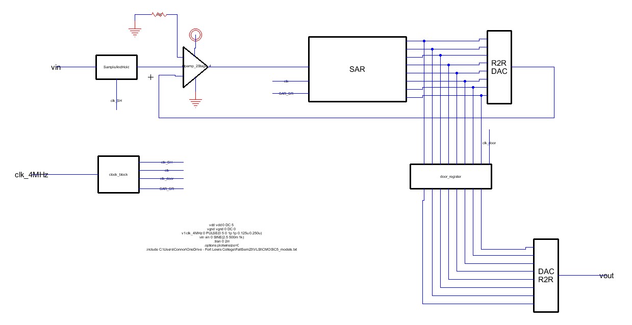
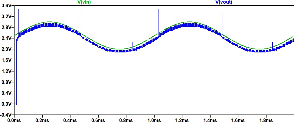
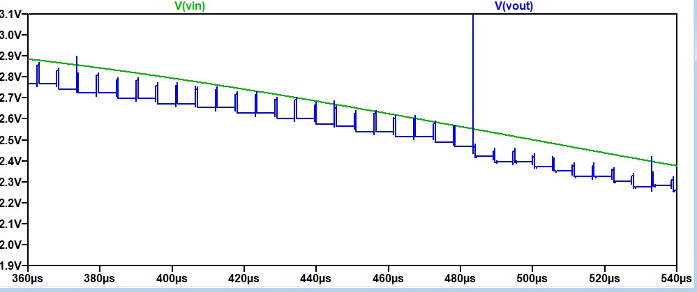
With all of the components together, we can finally build the 8-bit SAR ADC:


Results
Here is the simulation results of the TI DFF. The clock is fairly slow, thus the ouput (Q) is off.


Here is the simulation results of the SAR block. The simulation is an exact replica from Dr. Li's simulation in LTSpice.


Here is the simulation results of the Sample and Hold circuit: You can the it samples at the rising edge and holds the sample until the next rising edge.


Here is the simulation results of the Clock Register:


Here is the result of the final 8-bit SAR ADC:


Discussion
The functionality of all of the required circuits to built the SAR ADC are all exremely crucial to this final circuit. Although, the final R2R DAC is not necessary for production. It was only used to veryify the ADC functionality easily. You can see that we are able to recover the sine wave in the end. It is offset from the input, but this may be due to the resolution of the ADC.