1. Introduction
Logic gates are essential to the functionality of most circuits for digital electronics. They give us the ability to efficiently perform tasks on a conditional basis. It is crucial for someone in the semi-conductor industry to know how to design and layout these FET circuits. Out of the various logic gates that exist, the ones that are focused on in this lab are the NAND, NOR, and XOR gates. We will then use these gates in combination with the NOT gate we made in the previous lab to design a Full Adder.
3. Procedure
To begin, I created a schematic cell called "NAND{sch}" in Electric VLSI, and I laid out a NAND gate circuit with two NMOS and two PMOS transistors as seen in Figure 1 below. I then created an icon view from the schematic, called "NAND{ic}," and designed it to look like a NAND gate symbol. I ran a DRC test to make sure there were no errors present before creating a schematic called "sim_NAND{sch}" for a SPICE simulation as seen in PDF 1.
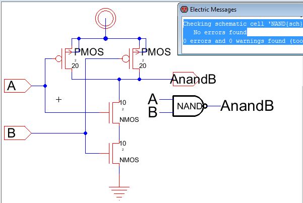
Figure 1. This is a screensnip of the schematic for the NAND gate, "NAND{sch}", with the DRC results highlighted in blue. The figure also shows the respective icon.
Once the DRC reported no errors, I created the layout cell called "NAND{lay}," and I began designing the layout. I added two NMOS and two PMOS with their needed components, and I made the proper connections as seen in Figure 2. I then ran a DRC and NCC check on the layout to make sure there were no errors in the design.
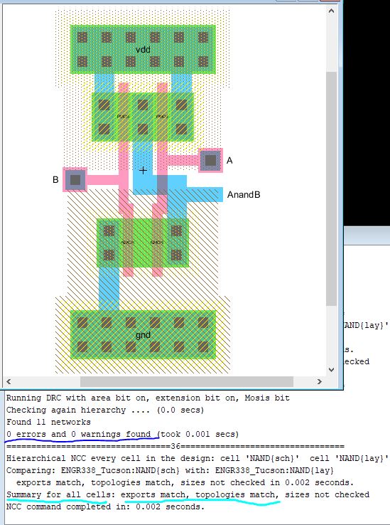
Figure 2. This is a screensnip of the layout of the NAND gate, "NAND{lay}", with the DRC results underlined in blue and the NCC results underlined in cyan.
Once the NAND gate design was confirmed to be error-free, I went on to design the NOR gate. I did so by repeating similar steps, but for a NOR gate instead. The schematic cell was called "NOR{sch}," and it is shown in Figure 3 with the icon from "NOR{ic}". I also created a schematic called "sim_NOR{sch}" to perform a SPICE simulation as seen in PDF 1. The layout cell was called "NOR{lay}," and it is shown in Figure 4 with the DRC and NCC results.
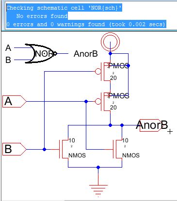
Figure 3. This is a screensnip of the schematic for the NOR gate, "NOR{sch}" with the DRC results highlighted in blue. The figure also shows the respective icon.
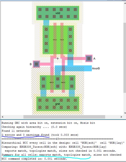
Figure 4. This is a screensnip of "NOR{lay}" with the DRC results highlighted in blue. The figure also shows the layout of the circuit with the proper connections.
After the NOR gate design was completed, I went on to create a XOR gate in the same fasion I created the NAND and NOR gates. The schematic cell was called "XOR{sch}," and it is shown in Figure 5 with the icon from "XOR{ic}". I also created a schematic called "sim_XOR{sch}" to perform a SPICE simulation as seen in PDF 1. Before moving on to the layout, I drew a stick diagram to plan out how I was going to put everything down. The layout cell was called "XOR{lay}," and it is shown in Figure 6 with the DRC and NCC results.
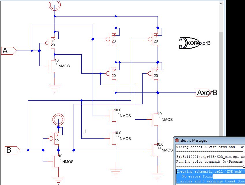
Figure 5. This is a screensnip of "XOR{sch}" with the DRC results highlighted in blue. The figure also shows the circuit of the XOR gate and its respective icon.
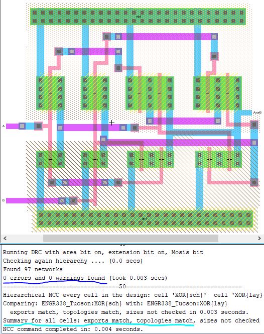
Figure 6. This is a screensnip of "XOR{lay}" with the DRC results underlined in blue, and the NCC results underlined in cyan. The figure also shows the layout of the circuit with the proper connections.
Once the XOR gate design was completed, I went to create a layout for a Full Adder. I did this in a similar fashion to how I designed the XOR gate. The schematic cell was called "Full_Adder{sch}," and it is shown in Figure 7 with the icon from "Full_Adder{ic}". I also created a schematic called "sim_FA{sch}" to perform two SPICE simulations as seen in PDF 1. The simulations were of Cin connected to ground, and then Cin connected to VDD. The layout cell was called "Full_Adder{lay}," and it is shown in Figure 8. This circuit was a bit crazy to look at when designing the layout.
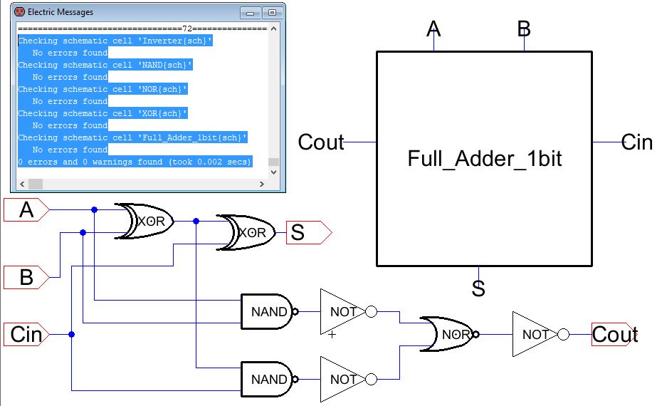
Figure 7. This is a screensnip of the schematic for a Full Adder, "Full_Adder{sch}", with the DRC results highlighted in blue. The figure also shows the respective icon.
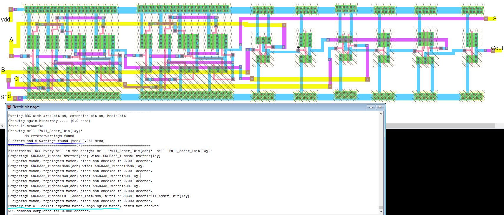
Figure 8. This is a screensnip of the layout for the Full Adder, "Full_Adder{lay}", with the DRC results underlined in blue and the NCC results underlined in cyan.
4. Results
The DRC and NCC checks all came back reporting 0 errors and all of the cells matching the cells in their respective cell groups. Below is a PDF of the various simulation, DRC, and NCC results that were not shown in-line above.
PDF 1. This PDF is a collection of screensnips of the various simulation results that were not shown in-line above. The figures are labeled.
5. Discussion
I think this lab would have required a lot more time than it did if it weren't for being required to build an XOR gate and a full adder in homework 5. The homework served useful since I made the schemtaics and icons for the NAND and NOR gates when doing the homework (as to practice implementing good habits by designing reusable blocks). This allowed me to really focus on the layout of each gate and put the extra time into making sure I understand why we layout the transistors the way we do and becoming more familiar with stick diagrams.
This lab was very enriching. I enjoyed getting a better understanding while doing this lab. I hope to get better at routing the wires efficiently with more practice in the future.