1. Introduction
Metal-Oxide Semiconductor Field-Effect Transistors (MOSTFETs) are popularly used in the semiconductor industry. These are transistors that use silicon doped with either phosphorous or boron with source, gate, and drain terminals. The two types of MOSFETs that are designed in this lab are the N-Well and P-Well transistors.
Knowing what these two transistors consist of and how they function together is crucial to being successful in the semiconductor industry. In this lab, a pMOS and nMOS will be designed and laid out in Electric VLSI. To further understand what is going on, the Current-Voltage Characteristic Curves (I-V curves) are simulated to ensure the design is functional and created properly.
3. Procedure
To begin, I opened up the Electric VLSI and the ENGR338 library from the last lab. I created a new schematic called "NMOS_IV{sch}," and I added a NMOS node to the schematic. I then edited the width and length, and I formatted the text as shown in Figure 1. I then changed the SPICE-model text to match what is in the C5_models.txt file. I then created a new schematic called "PMOS_IV{sch}," and I added a PMOS node to the schematic. I edited the width and length as I did with the NMOS, and I formatted the text as shown in Figure 2.
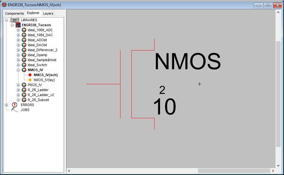
Figure 1. A screen-snip of the schematic for NMOS_IV{sch}. The width of the transistor has been set to 10 lambda, and the length has been set to 2 lambda. The format of the text has been altered from the default format.
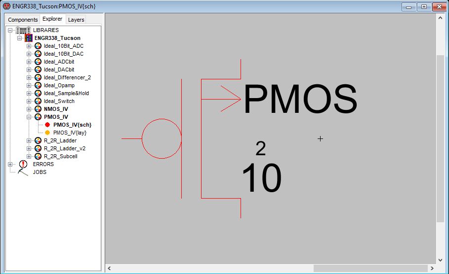
Figure 2. A screen-snip of the schematic for PMOS_IV{sch}. The width of the transistor has been set to 10 lambda, and the length has been set to 2 lambda. The format of the text has been altered from the default format.
I then created layout views for each schematic. Starting with the "NMOS_IV{lay}," layout view, I placed down an nMos Node and renamed it to match what is in the "C5_models.txt" document. I then added two nAct Nodes for the source and drain terminals. I then placed the metal1-to-poly1 contact for the gate terminal. After, I placed a pWell Node for the body connection. I resized the nodes as follows: nMos Node width changed to 10 lambda; nAct Nodes x dimension changed to 10 lambda; pWell Node x dimension changed to 10 lambda. I then moved the components and made the connections as shown in Figure 3. To do this, I went through a series of DRC and ERC checks to ensure there were no issues along the way. This process is documented as shown in PDF 1.
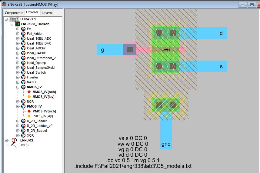
Figure 3. A screen-snip of the final layout with SPICE simulation code and connections for NMOS_IV{lay}.
PDF 1. This PDF consists of the DRC and ERC results that were perfomed in the process of designing the layout for "NMOS_IV{lay}". They are in order of first task performed to last task performed.
I then went to the layout view called "PMOS_IV{lay}" to design the PMOS layout. I added a pMos Node and renamed it to match what is in the "C5_models.txt" file. I then added two pAct Nodes, one for the drain and one for the source, and an nWell Node. I also added a metal1-to-poly1 contact for the gate terminal. I rearranged the components as shown in Figure 2. I changed the sizes of the componets as I did for the NMOS. I also changed the nWell Node size in the y dimension to 6 lambda after recieving the well check error shown in PDF 2. After this error was corrected, I made the proper connections, and I did a DRC and ERC check to ensure it was error-free.
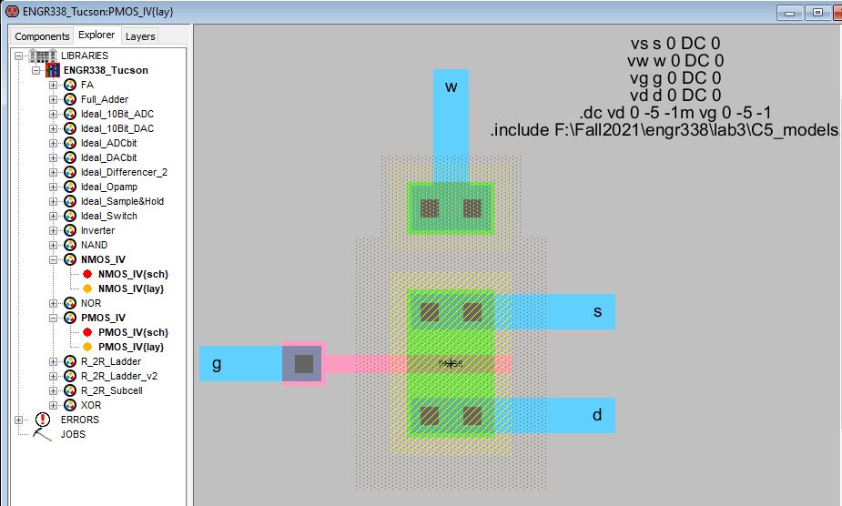
Figure 4. A screen-snip of the final layout with SPICE simulation code and connections for PMOS_IV{lay}.
PDF 2. This PDF consists of the DRC and ERC results that were perfomed in the process of designing the layout for "PMOS_IV{lay}". They are in order of first task performed to last task performed.
I then ran the simulations for both the "PMOS_IV{lay}" and "NMOS_IV{lay}" in LTSpice. I then copied the codes to their respective schematics. I completed the connections in the schematic by adding the ground component to the body connection and nodes to the terminals as shown in Figures 5 and 6. I then labeled the terminals to match the code, and I ran the simulations for both MOSFET schematics.
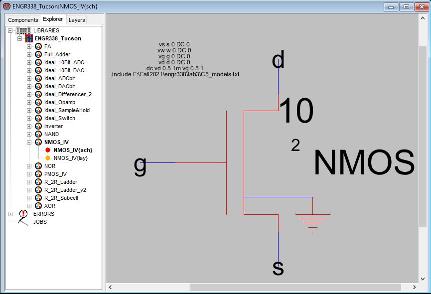
Figure 5. A screen-snip of the final connections for NMOS_IV{sch} SPICE simulation.
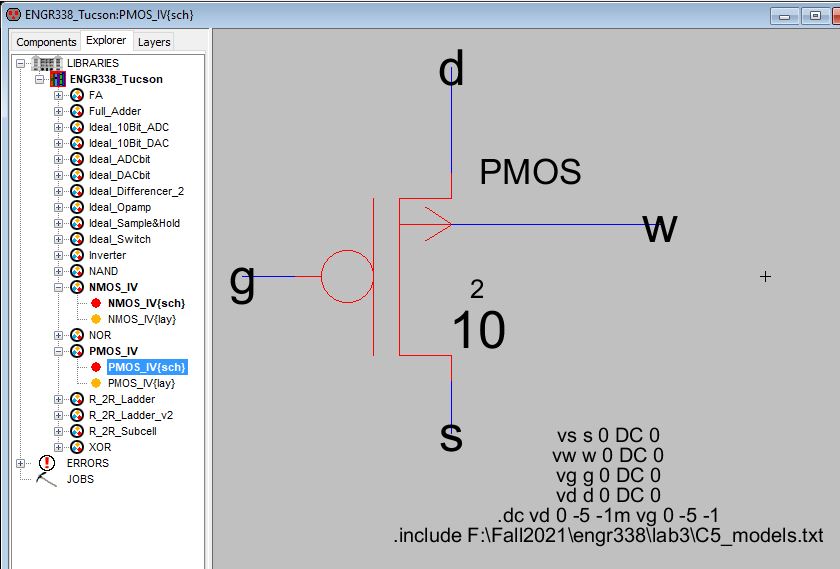
Figure 6. A screen-snip of the final connections for PMOS_IV{sch} SPICE simulation.
5. Discussion
The simulated results were as to be expected, and the IV curves from the layout simulations match their respective schematic simulation IV curves. This lab gave me more insight to how the inner-workings of the PMOS and NMOS MOSFETs function. I also gained the skill of designing a MOSFET layout in VLSI software, and I learned skills that will become good habits in the future as I layout more designs in my career.