1. Introduction
Converting signals from analog to digital is a fundamental skill that is crucial to effectively designing a circuit with many different types of components. Knowing the circuitry of these semiconductors is not only important to know if entering the semiconductor industry, but also important for better understanding how a design functions when these components are involved.
Being familiar with how VLSI software works is also an important skill to have if entering the semiconductor industry. Many start-up companies use Electric VLSI software because it is open source. Many larger companies use more expensive programs like Cadence; however, the general concepts learned with Electric VLSI can be applied to the other softwares being used in the industry.
In this lab, a circuit for a R-2R Digital-to-Analog Converter is designed in Electric VLSI and simulated in LTSpice. This is to give us a feel for using a VLSI software as well as giving us a chance to apply what we have learned about the R-2R DAC structure.
3. Procedure
To begin this lab, I went through the installation process for Java and Electric VLSI due to using a different device this semester. I then linked Electric to LTSpice, and I downloaded the .jelib library provided for this lab. I then copied the simulation, and the cells needed for it, to my own library I created specifically for this class. I then opened the schematic titled "sim_ADC_DAC{sch}" and ran the simulation in LTSpice.
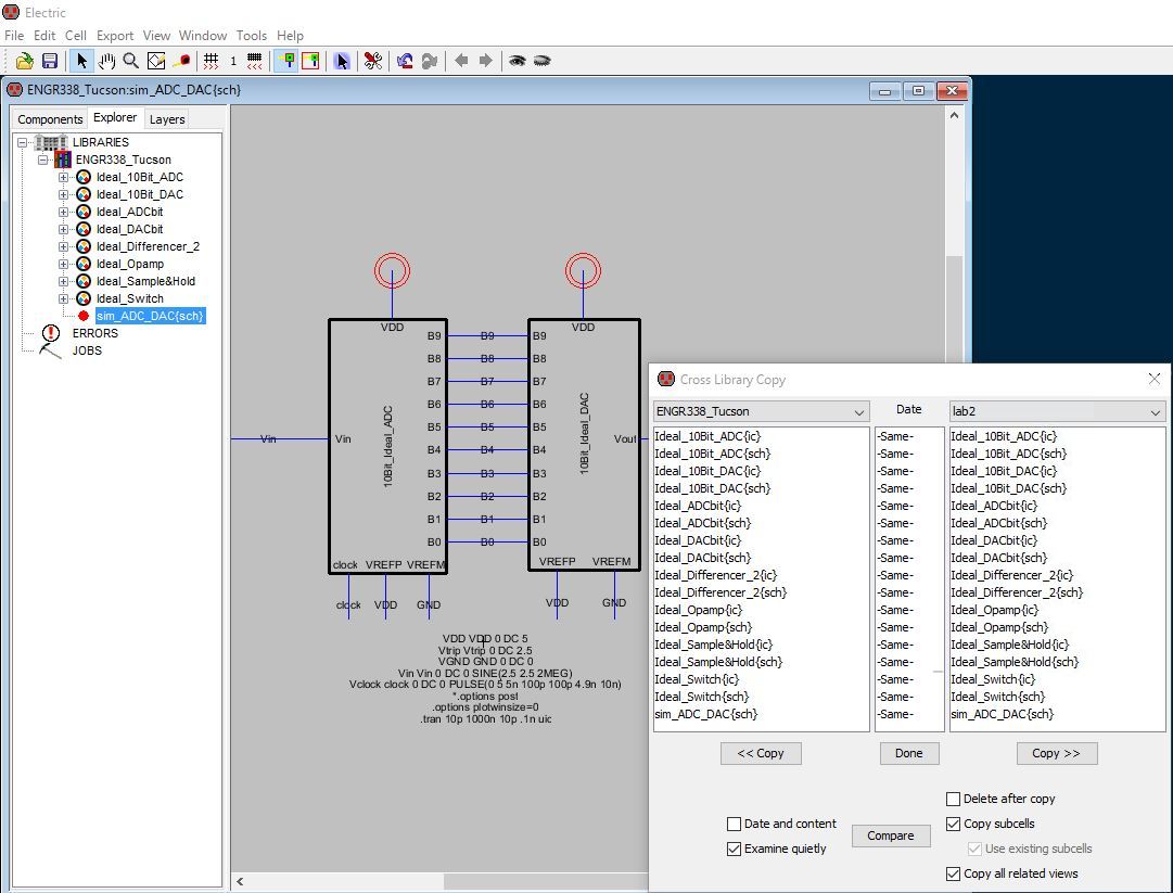
Figure 1. This is a screen-snip of the files copied from the library provided for this lab to the library I created for this class, ENGR338. The schematic is "sim_ADC_DAC{sch}" that was opened from the ENGR338 library.
The schematic shows an ideal 10-bit ADC wired to an ideal 10-bit DAC.
Next, I designed a R-2R DAC circuit in a schematic cell in Electric VLSI. I ran a DRC test on the circuit, and designed an icon for this DAC after the DRC results came back with no errors.
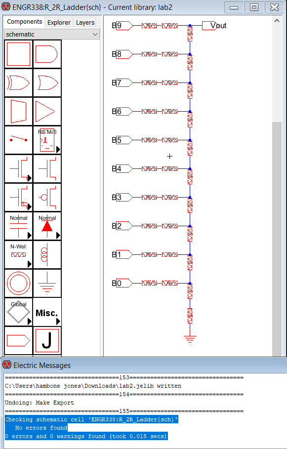
Figrue 2. This is a screen-snip of the 10-bit R-2R circuit schematic, icon, and DRC report results. The results are highlighted in blue.
The circuit consists of 10K Ω N-well resistors, pins, and the ground (GND) component.
After the icon was designed, I duplicated the "sim_ADC_DAC{sch}" and renamed it "sim_ADC_R_2R_DAC{sch}" and replaced the ideal DAC with the R-2R DAC that was just designed, and then I ran the simulation in LTSpice.
The final thing I did for this lab was test the time delay from the B9 pin when the DAC drives a load of a 10pF capacitor. To do this, I first found the Thevenin's Equivalent circuit of the R-2R ladder to estimate the output if a power source that is pulsing between different voltage potentials, then I altered the circuit and the SPICE code, and I ran the simulation in LTSpice to confirm the calculations.
Figure 3. This is a PDF containing the altered circuit and SPICE code, and the hand calculations for the Thevenin's Equivalent circuit used to predict the time delay at B9.
4. Results
The simulated output from the ideal ADC-DAC circuit is seen in Figure 4, and it shows the analog input plotted with the digital output. The simulated output for the circuit of the ideal ADC with the R-2R DAC are seen in Figure 5, and it also shows the analog input plotted with the digital output.
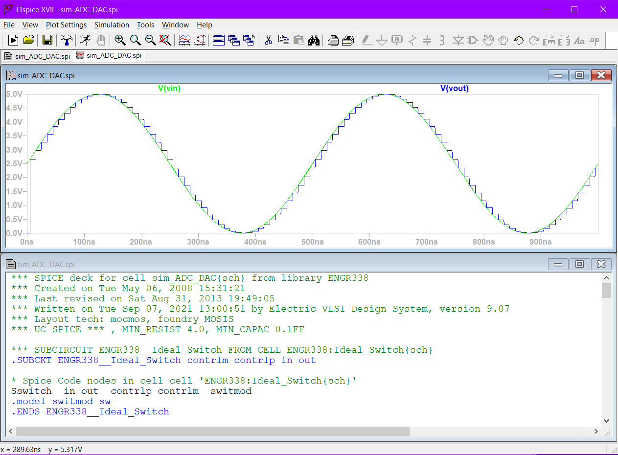
Figure 4. This is a screen-snip of the results of the LTSpice simulation for the circuit with the ideal DAC. The analog input, in purple, is plotted with the digital output, in green.
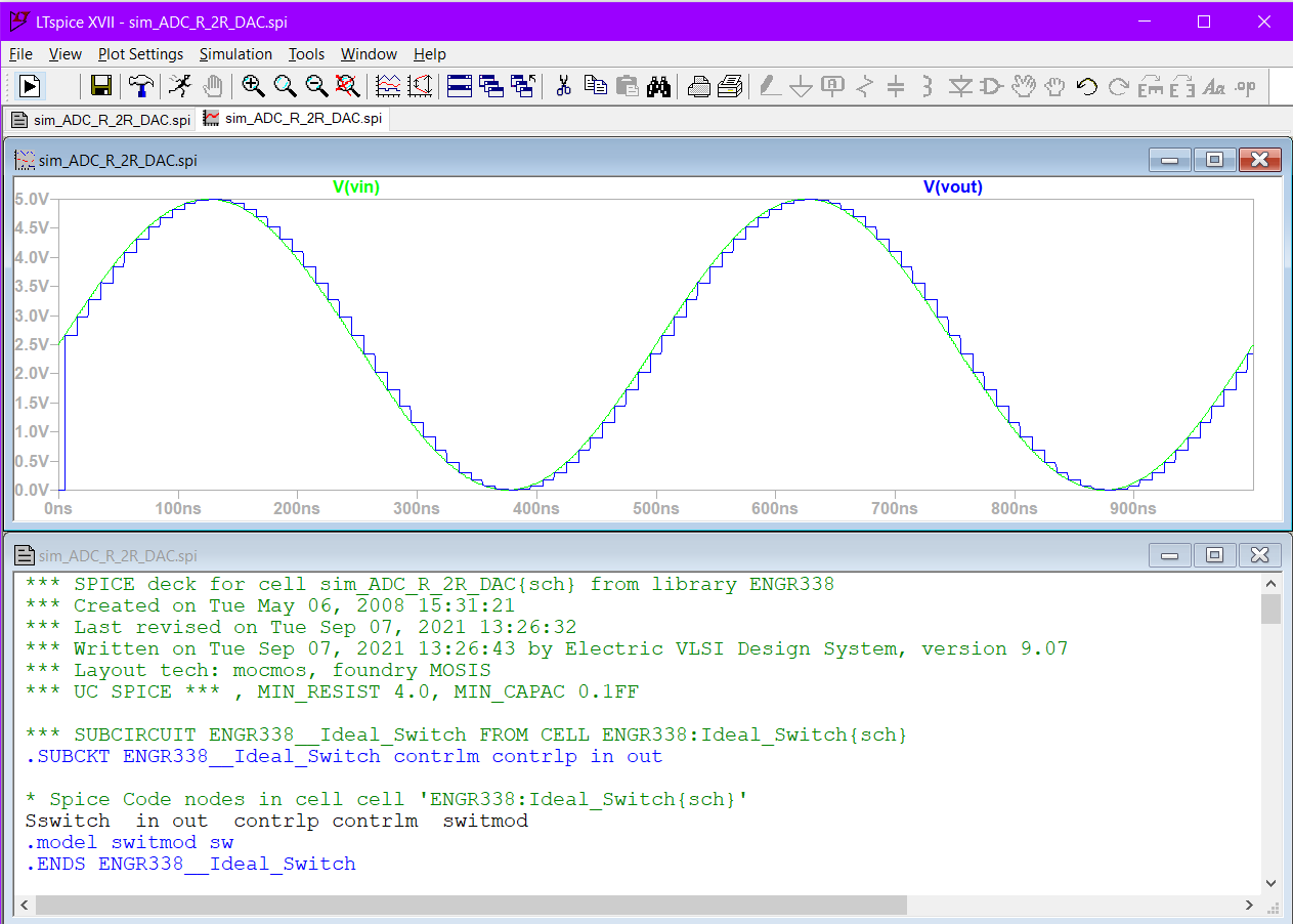
Figure 5. This is a screen-snip of the results of the LTSpice simulation for the circuit with the R-2R DAC created during the lab. The analog input, in purple, is plotted with the digital output, in green.
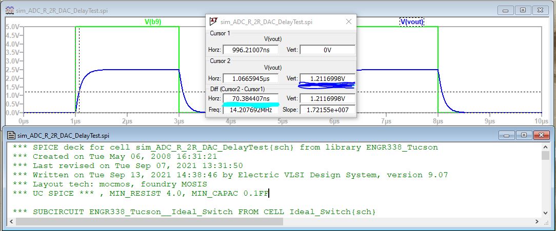
Figure 6. This is a screen-snip of the results of the LTSpice simulation for the DAC delay-time test The graph represents the voltage potential of the load being driven by the R-2R DAC.
The cursors are aligned to show that the time delay is consistent with the hand calculations. The time difference reads 70.38 nanoseconds, highlighted in cyan, and the voltage level at that time reads at 1.21V, highlighted in blue.
Note the cursor is not aligned exactly at 1.25V mark.
In Figure 6, the voltage potential of the capacitor is plotted with the input pulsing voltage. The output values are consistent with the hand calculations. The time difference and voltage level at that time are highlighted in cyan and blue. Note the cursor is not aligned exactly at 1.25 V mark and reads 70.38 nanoseconds. I could not get the cursor to align at exactly 1.25 V.
5. Discussion
The results for the tasks were as to be expected. The simulation results shown for the time-delay test would have directly verified the calculations if the cursors would have been positioned in the exact spot needed. The cursor at 1.21V shows a reading of 70.38 nanoseconds. This lab provided good refresher experience with Electric VLSI, designing circuits with resistive transistors, and understanding the graphs from the SPICE simulations.