ENGR338 SPRING 2021
Lab 4: MOSFETs and IV Curves
Name: Caroline Kleven
Email:
cekleven@fortlewis.edu
1. Lab 4: MOSFETs and IV Curves
For Lab 4, we had two objectives:
1. Be able to build MOSFETs in Electric VLSI
2. Be able to run simulations to analyse the IV curves of the MOSFETs
2. Introduction
During this lab, we completed three tasks:
1. Created schematics of NMOS and PMOS 4 port MOSFET transistors
2. Created layouts for our schematics
3. Ran a simulation of our layouts in LTspice
3. Materials and Methods
For Lab 4 we used:
1. Electric VLSI, to build schematics and layouts of MOSFETs
2. LTspice, to run simulations
4. Results
To begin our first task, we created a schematic of an NMOS device, saving it as a C5 model.
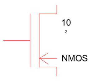
Fig. 1: Schematic of NMOS device in Electric VLSI
We did the same for a PMOS device.
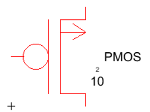
Fig. 2: Schematic of PMOS device in Electric VLSI
For our second task, we then created a layout for our NMOS device, saving it as a C5 model once again.
We exported the pins of each arc, being sure to check our layout for any errors before moving on.
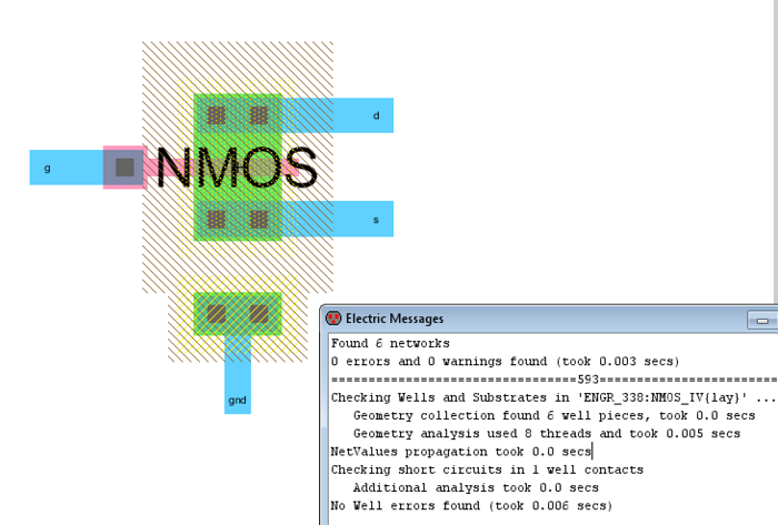
Fig. 3: NMOS layout in Electric VLSI, checked for errors
We did the same for our PMOS device.
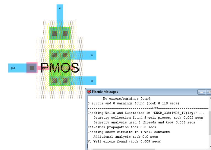
Fig. 4: PMOS layout in Electric VLSI, checked for errors
We added LTspice code to our PMOS layout to begin our third task.
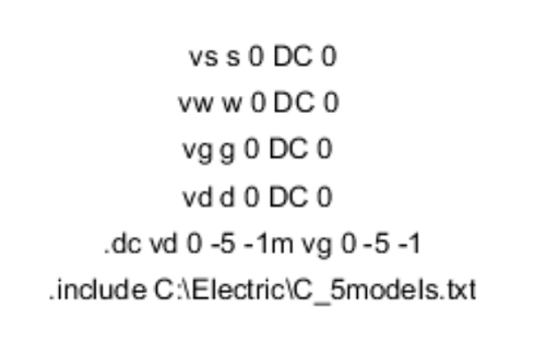
Fig. 5: LTspice code added to our PMOS layout in Electric VLSI
We then wrote the Spice Deck in order to view the source current of the PMOS device.
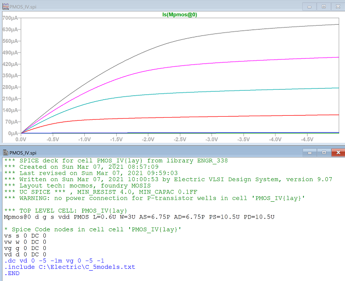
Fig. 6: LTspice plot of the source current of the PMOS device
We added a similar code to the layout of the NMOS device.
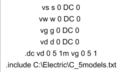
Fig. 7: LTspice code added to our NMOS layout in Electric VLSI
And wrote the Spice Deck once again, in order to view the source current of the NMOS device.
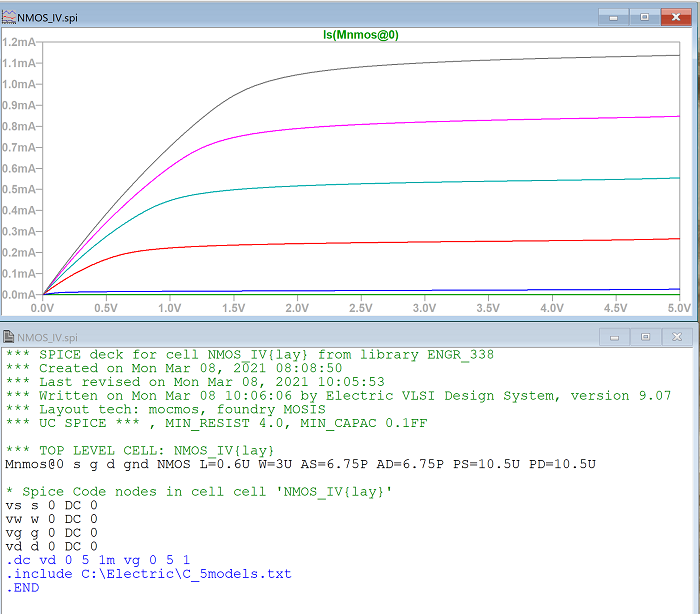
Fig. 8: LTspice plot of the source current of the NMOS device
To ensure our schematics matched our layouts, we added the same
exported pins, the spice code from the layouts, and a ground node to
our NMOS and PMOS schematic cells, respectively. We made sure they
passed both DRC and NCC checks.
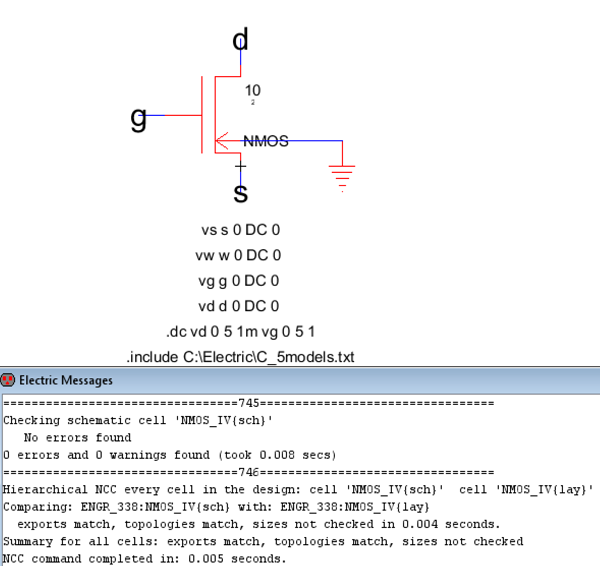
Fig. 9: PMOS schematic made to match the PMOS layout in Electric VLSI, checked for errors
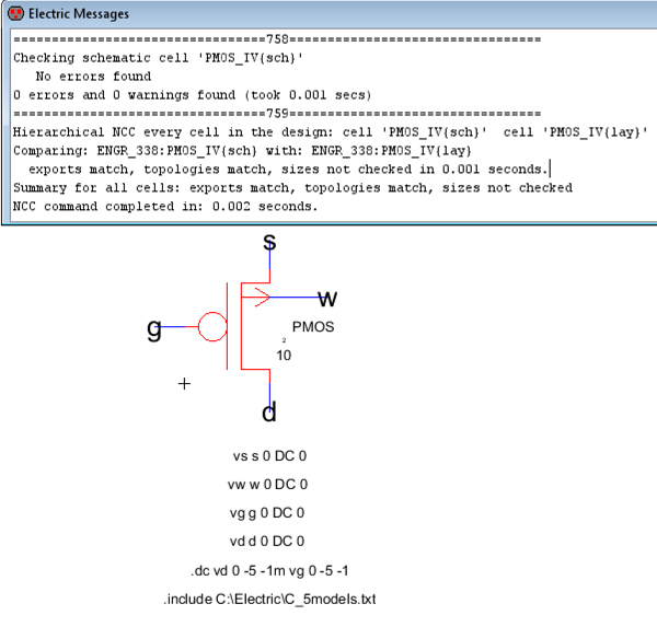
Fig. 10: PMOS schematic made to match the PMOS layout in Electric VLSI, checked for errors
We then simulated the schematics in LTspice, to verify that they created the same plots of the source currents.
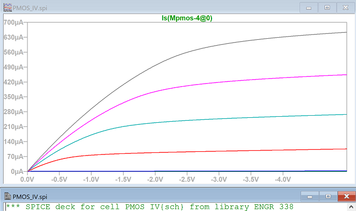
Fig. 11: PMOS schematic simulated in Electric VLSI
5. Discussion
This lab helped me become faster at creating schematics and layouts,
and I enjoyed learning more about how Electric VLSI and LTspice can be
used together.