ENGR338 Spring 2021
Lab 2: Design an R-2R DAC
Name: Caroline Kleven
Email: cekleven@fortlewis.edu
1. Lab 2: Design an R-2R DAC
For Lab 2, we had three objectives:
1. Understand the operation of the ideal ADC and DAC
2. Design a R-2R DAC in Electric VLSI to replace the ideal DAC
3. Become familiar with Electric VLSI and LTspice for integrated circuit
design
2. Introduction
During this lab, three tasks were completed:
1. Copying existing ideal ADC-DAC files to our own library in Electric VLSI and running a simulation on LTspice
2. Building a schematic of an R-2R DAC on Electric VLSI and running a simulation on LTspice
3. Testing a time delay from a specific pin when the DAC schematic we built drives a 10pF load
3. Materials and Methods
For Lab 2 we used:
1. Electric VLSI, to build schematics
2. LTspice, to run simulations
4. Results
For our first task, we copied existing ideal ADC-DAC files to our own library in Electric VLSI.
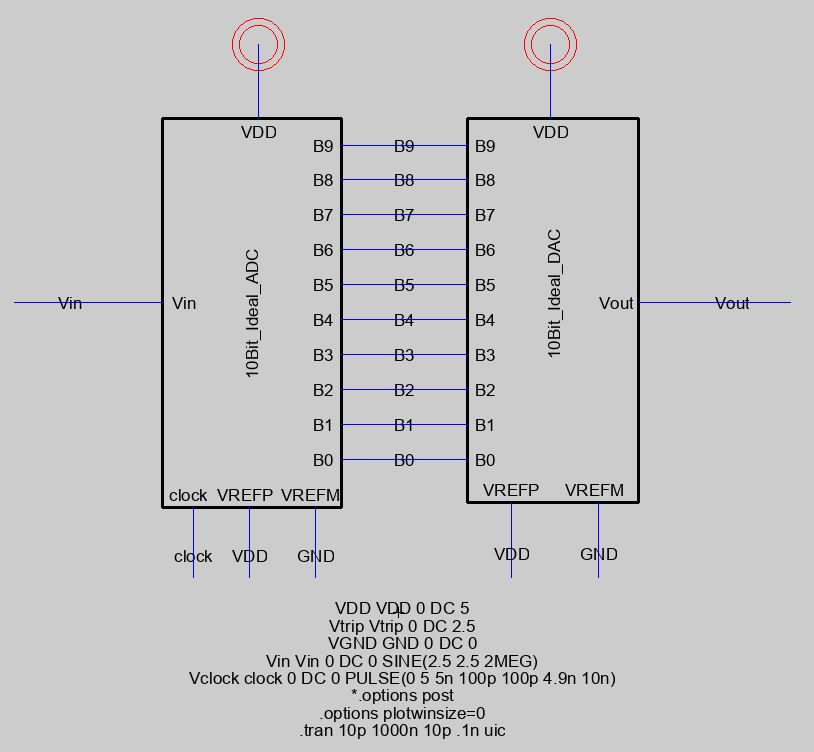
Fig. 1: Ideal ADC-DAC schematic
We then ran a simulation on LTspice to show the analog (Vin) and digital (Vout) signals.
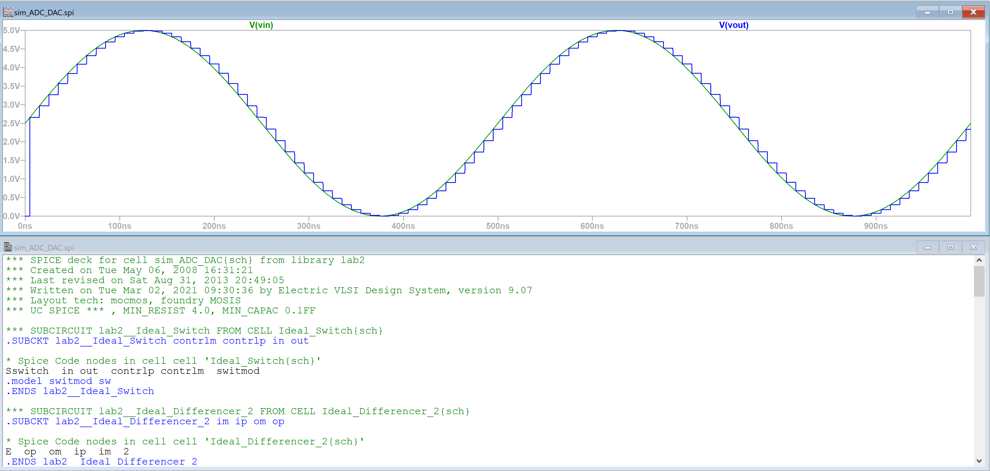
Fig. 2: LTspice simulation of existing ideal ADC-DAC files
For our second task, we first built a schematic of an R-2R DAC on Electric VLSI.
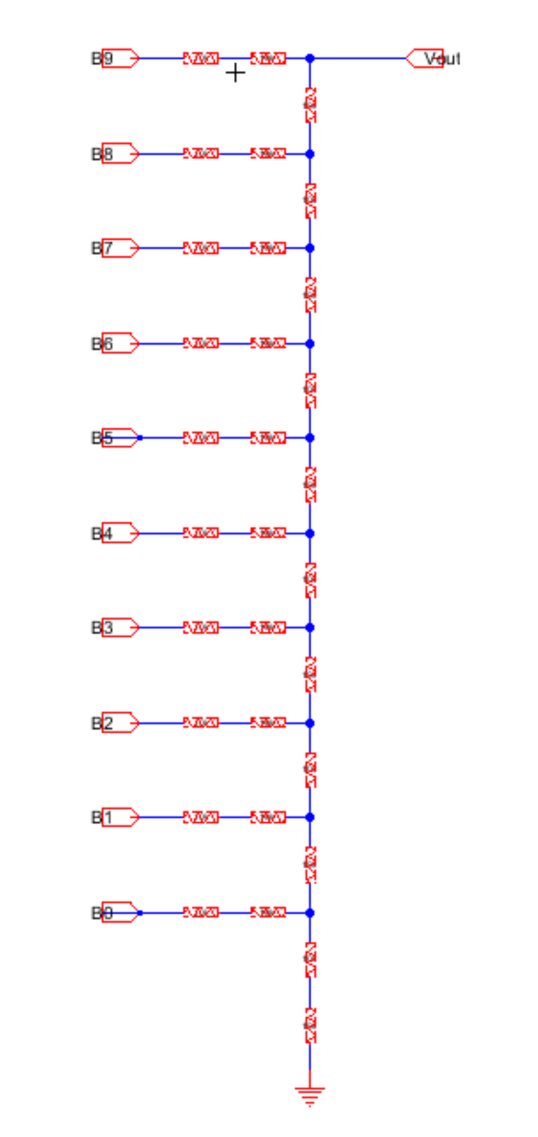
Fig. 3: schematic of R-2R DAC on Electric VLSI
We then checked to ensure there were no errors in our work.
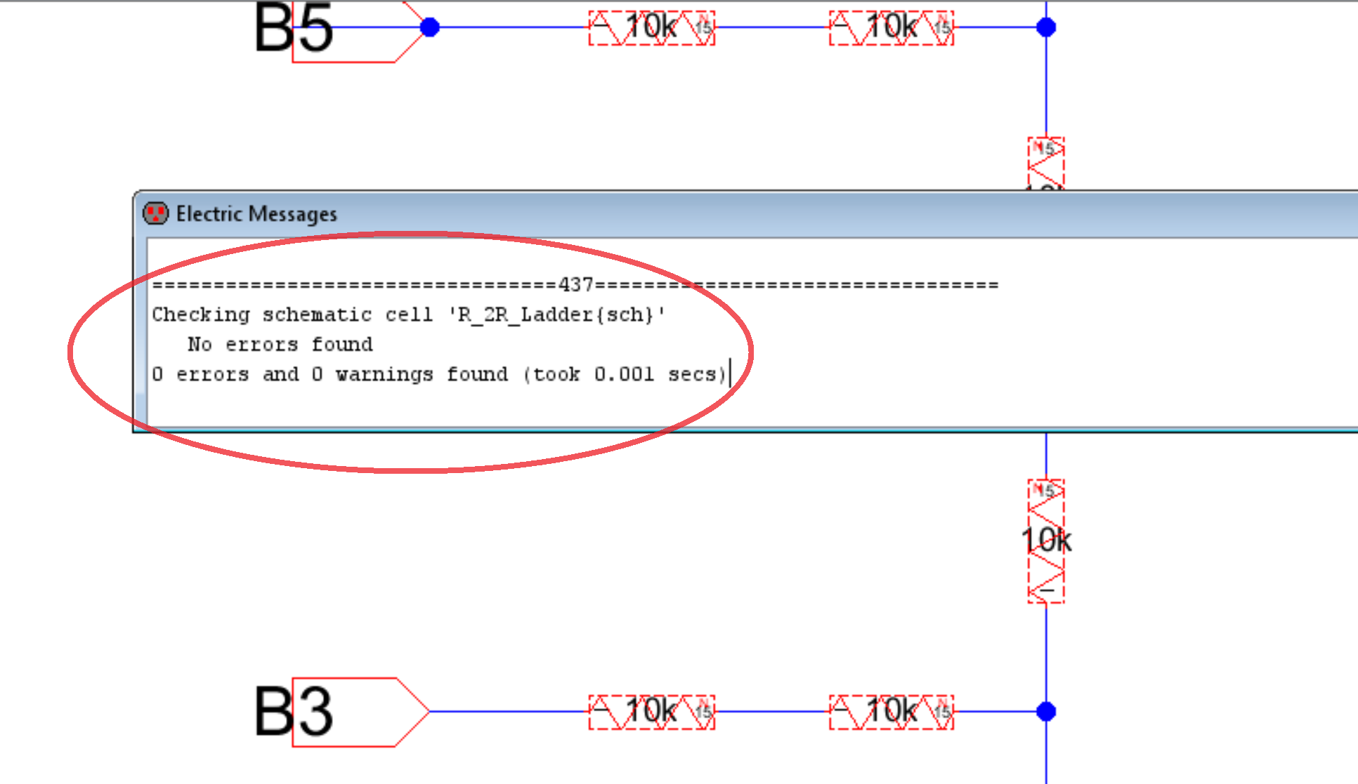
Fig. 4: Checking for errors in our R-2R DAC schematic on Electric VLSI
After verifying there were no errors, we made an icon using our schematic.
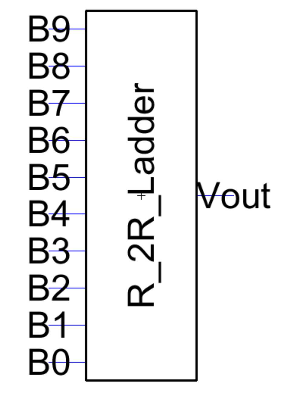
Fig. 5: R-2R Ladder icon made with our schematic on Electric VLSI
We then replaced the original ideal DAC with our R-2R DAC
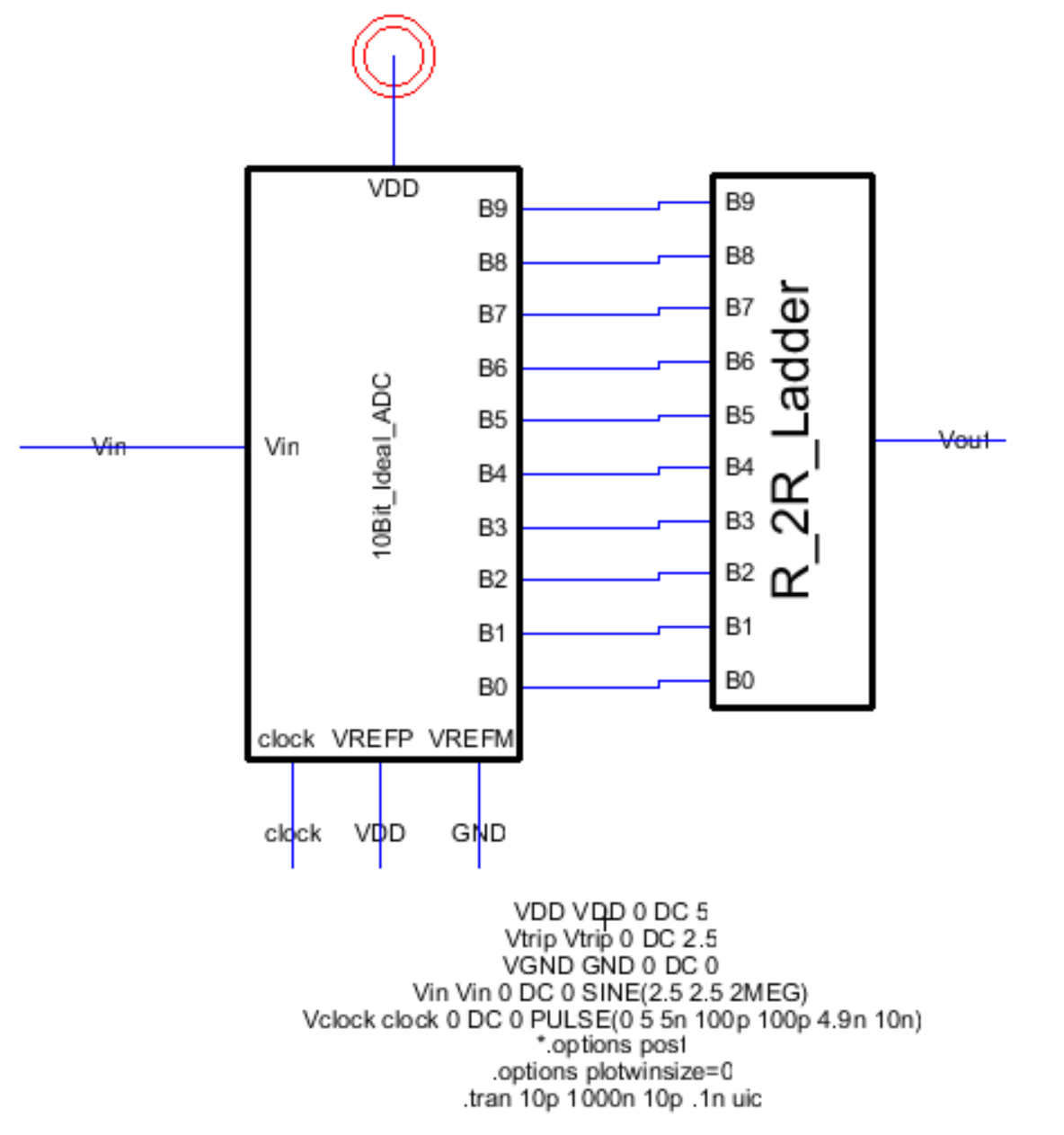
Fig. 6: R-2R Ladder icon replacing the original 10 bit ideal DAC on Electric VLSI
We then ran a new simulation on LTspice.
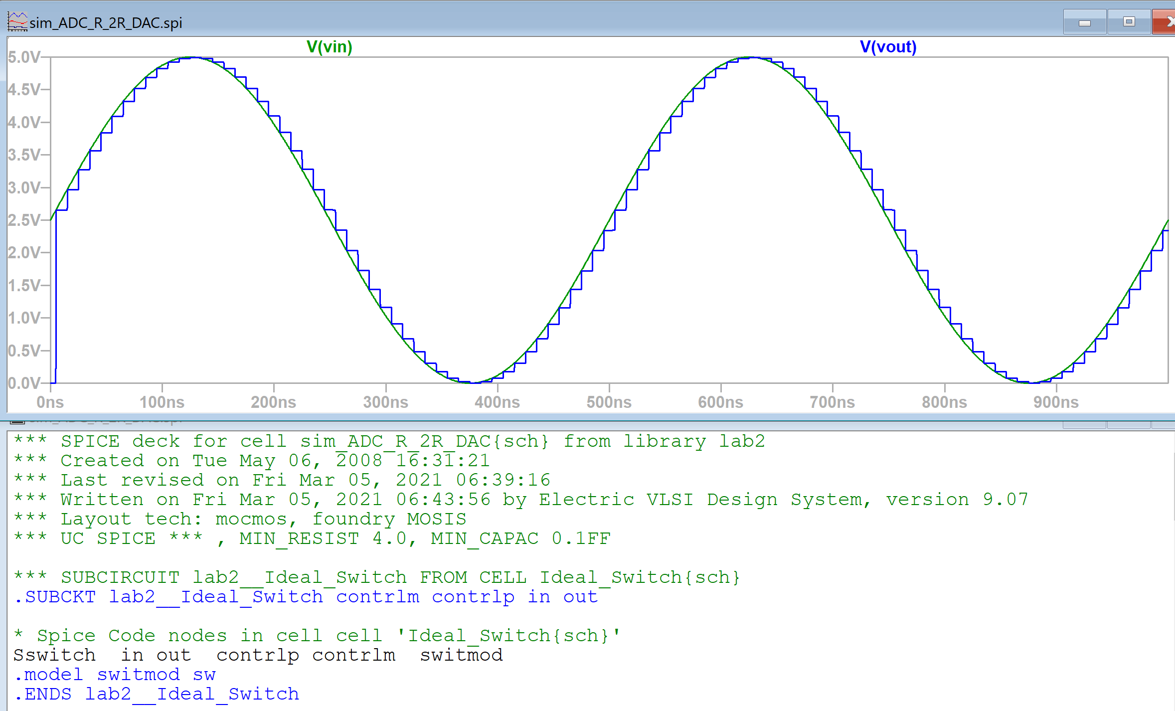
Fig. 7: LTspice simulation with our R-2R Ladder replacing the original 10 bit ideal DAC
The new R-2R Ladder simulation is nearly identical to the original simulation run with the existing ideal DAC.
Our third task was to test a time delay from a pin B9 on the DAC schematic we built, driving a 10pF load.
We accomplished this by first grounding pins B0 - B8, and adding a 10pF load to the output, checking for errors.
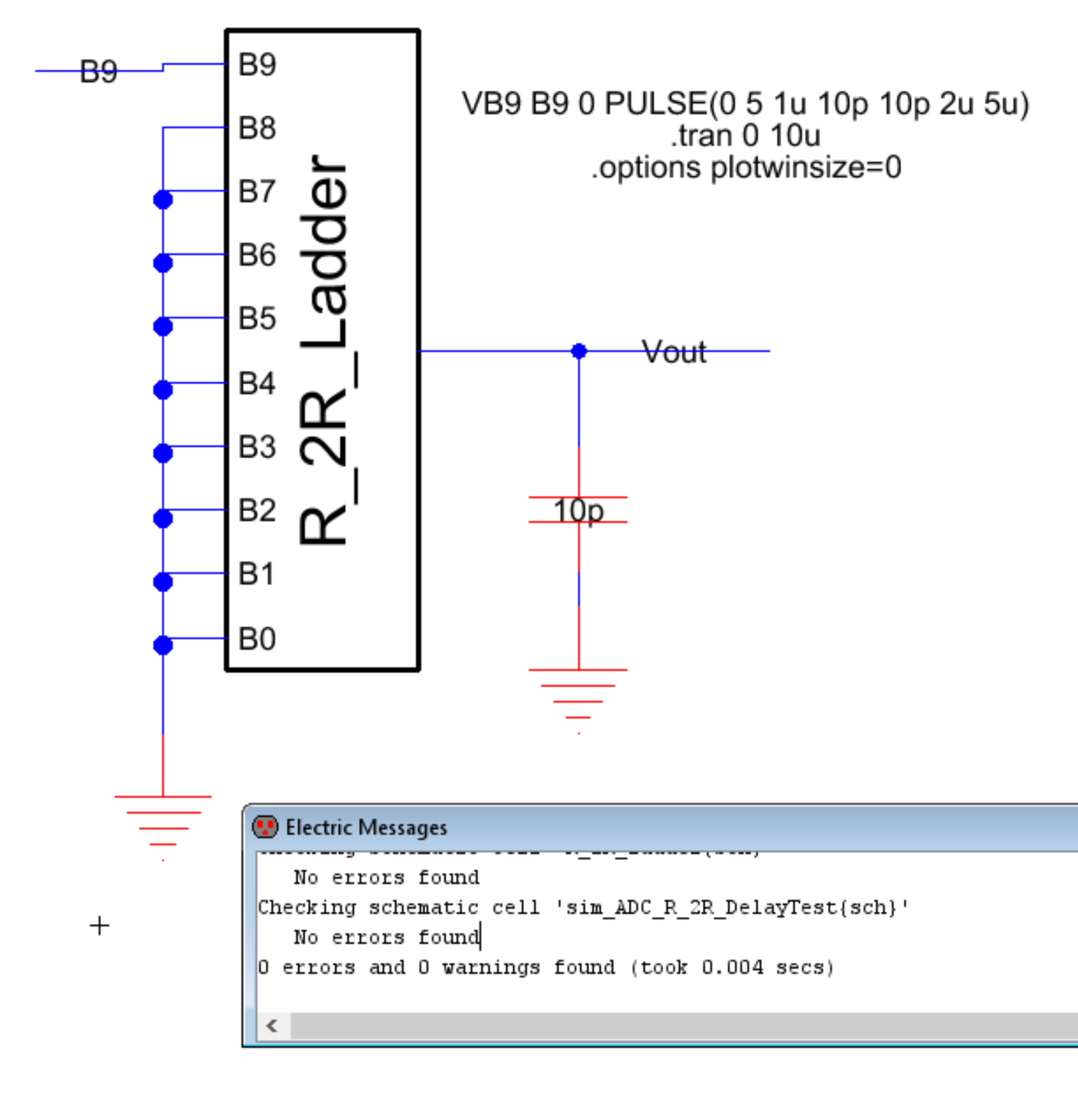
Fig. 8: R-2R Ladder schematic on Electric VLSI with a 10pF load, displaying no errors
We know that our final pulse should be 2.5V, based on the Thevenin equivalent circuit.
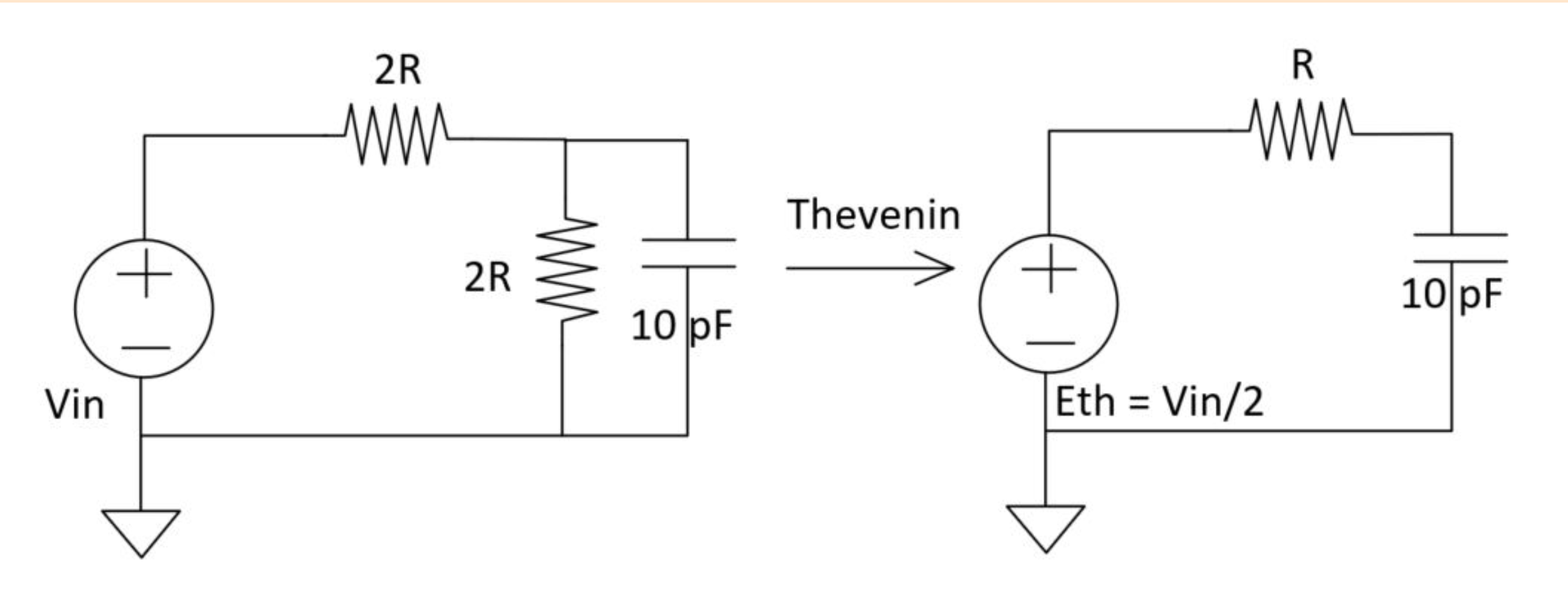
Fig. 9: Thevenin equivalent of the R-2R ladder with a 10pF load
When we use the 0.7RC equation, we calculate that 0.7RC*10k*10pF = 70ns
We can also calculate Vin/2 = 2.5/2 = 1.25V
We then run a new simulation on LTspice, which we probe at 1.25V.
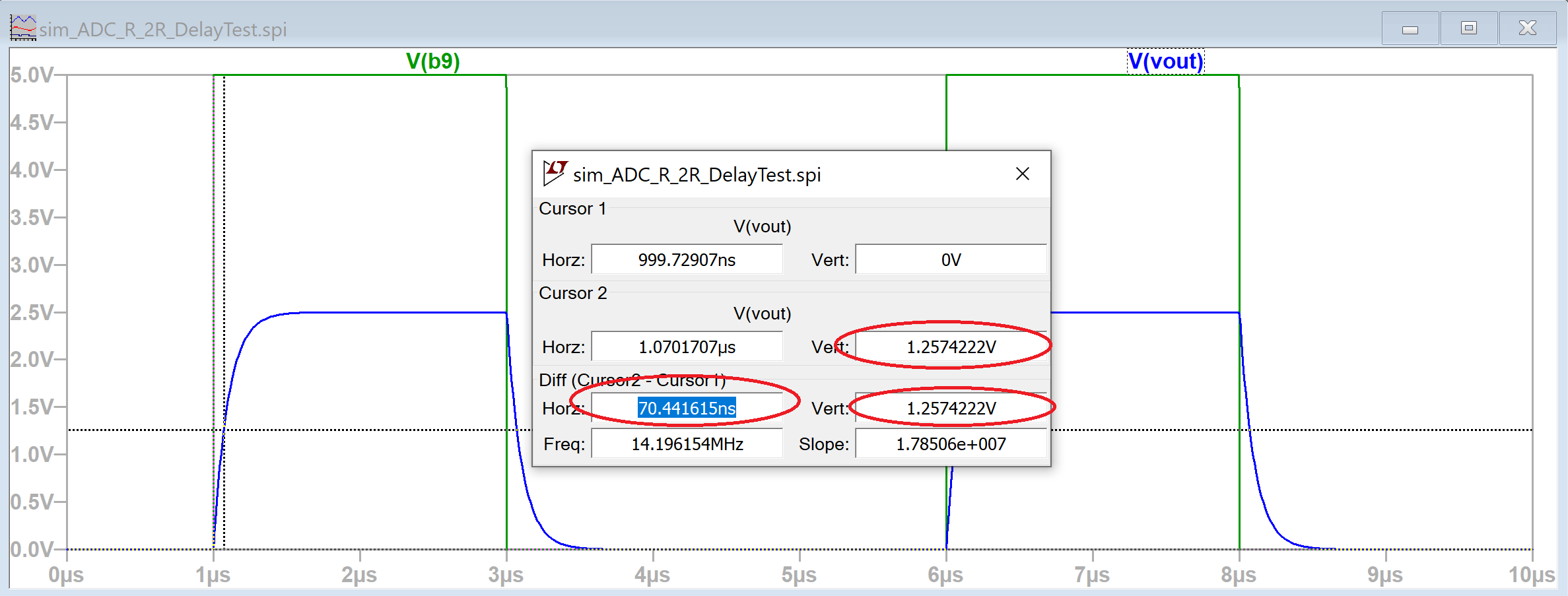
Fig. 10: LTspice simulation of our R-2R schematic running a 10pF load
We can see that our simulation verifies that our time delay calculations were correct.
5. Discussion
I feel like I have a much better understanding of how to operate both LTspice and Electric VLSI after completing this lab.