ENGR337 Lab 2020 Spring
Project
Name: Jesse Duran
Email: Jiduran@fortlewis.edu
1. Complete Op Amp IC
2. Introduction
This project was to create an Operational Amplifeir
complete with ESD protection using Electric VLSI. This is the
culmonation of our Analog Electronics course as a whole, bringing
together all that we have learned.
3. Materials and Methods
Electric VLSI was used to layout the IC and
schamatics.
4. Results


Figure 1. Bias Circuit Layout

Figure 2. Bias circuit icon and schematic.

Figure 3. Capacitor layout

Figure 4. Capacior schematic

Figure 5. Op Amp schematic
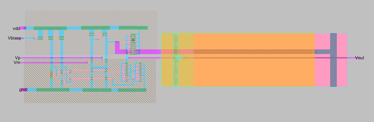
Figure 6. Op Amp Layout

Figure 7. ESD op amp schematic

Figure 8. ESD Layout

Figure 9. NCC passed and DRC passed
5. Discussion
This process exposed us to the proccess of laying out an IC chip. This
skill is hard to come by so it is valuable. Understanding how the chip
is constructed from the ground up reenforces the content we have
covered over this course. The trouble shooting practice in this layout
helped to cover all the bases of what is happening in each compant.