ENGR201 Lab 2018
Fall
Lab 7 Soldering and Capacitors.
Outcome
of this lab:
1.
Be able to do soldering independently.
2. Observe and analyze the voltage waveforms obtained when
charging/discharging a capacitor through a resistor.
3. Observe the frequency response of an RC low-pass filter and high-pass filter.
Instructions:
1. Before
soldering:
a.
Ensure adequate ventilation. If multiple people are soldering in a
concentrated area, set up a fan to gently blow fumes and vapors away
from you and your co-workers.
b. Keep area
clean around workplace at all times.
c.
When working with statically sensitive components (most active devices
such as ICs, FETs, transistors, etc.), be sure to use a anti-static mat
to work on and wear an anti-static wrist strap to minimize risk of
electrostatic discharge (ESD) damage. (Not sure if we will have this
ready in the lab this semester, link)
2. Tools
a.
Temperature-controlled soldering iron with fine tip (about 1/16" to
1/8" wide).
b. Rosin core
solder with a diameter of about 0.032" and a tin-lead (Sn-Pb) content
of about 60/40%.
c. A damp (not
dry!) sponge for keeping the tip of the soldering iron clean.
3. Soldering
a. Parts to be
soldered must be clean. Test the cleanness by pre-tinning wires before
soldering them together.
b. Whenever
possible, fix the parts to be soldered so that they are not moving
during and shortly after soldering.
c.
Make sure the tip of the soldering iron is clean! An oxidized tip will
not transfer enough heat for the solder to melt fast, but enough to
melt plastic and damage printed circuit boards.
d. Apply a small
amount of fresh solder to the tip of the soldering iron. Then heat the
parts to be soldered and apply solder to the parts (not the iron!)
until it melts. Do not move the parts until the solder has cooled down!
e. A good solder
joint looks shiny and bright silverish. Do not apply excessive amounts
of solder!
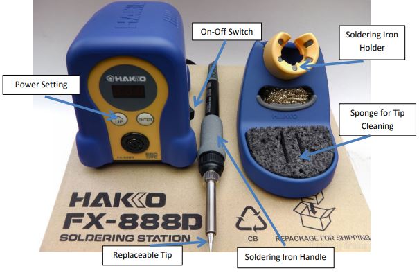
An
example of a soldering station I used in my graduate school. You may have a slightly different soldering iron, but just show
you the components of a typical soldering station:
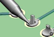
Minimal
thermal linkage due to insufficient solder between the pad and
soldering iron tip. A solder bridge provides thermal linkage to
transfer heat into the pad and component lead.
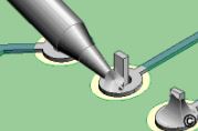
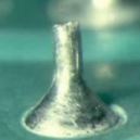
Solder blends to
the soldered surface, forming a small contact angle:
A good solder
joint is shown below:
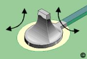
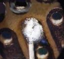
Cold Solder
Joints Joints that are dull or convex are potentially “cold” solder
joints. Cold solder joints DO NOT make a good electrical
or mechanical connection.
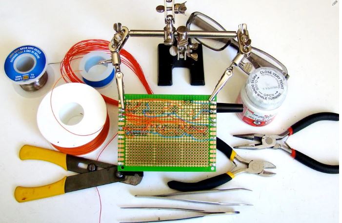
A
complete set of tools you will need for soldering (not including the
iron):
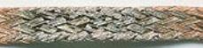
4. Use of Solder
Wick
a. Solder wick
is typically a ribbon of braided fine copper wire with rosin core flux
impregnated into it.
b. To use solder
wick, lay the wick over the joint to be de-soldered.
c. Apply the
heated tip of the soldering iron to allow the wick to be heated and
melt the solder in the joint.
d. The solder
will flow out of the joint and into the wick through capillary action.
5. Capacitors:
A
capacitor is a passive element designed to store energy in its electric
field. Capacitors are used extensively in electronics, communications,
computers, and power systems, e.g. in the tuning circuits of radio
receivers and as dynamic memory elements in computer systems. A
capacitor consists of two conducting plates separated by an insulator
(or dielectric), and is determined by the surface area of the plates,
the spacing between the plates and the permittivity of the material
(i.e. 𝐶 = 𝜖𝐴/𝑑), with a unit of farads (F).
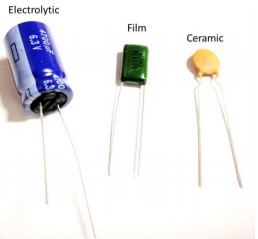
Three types of
capacitors:
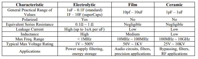
Characteristics
of the three main types of capacitors:
Tasks:
1. Watch the following two videos about soldering:
video
1
video
2
2. Build the folllowing circuit in LTSpice:
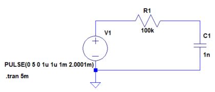
a. Explain the parameters in the PULSE() function.
b. Change the
values for R and C to: R=1k, C=100n; R=10k, C=10n; did you see any
differences in 'delay'? Why? How can you increase/decrease the delay?
(only in LTSpice)
c. Derive the equation to calculate the delay of the circuit and
compare to your simulation.
d.
Use R=100k, C=1 nF, build the circuit on a 'Prototype PCB (Universal
Printed Circuit Board)', use an oscilloscope to probe the input
&
output, and measure the delay. Compare your measurements to your
calculation and simulation (organize the calculation, simulation, and
measurement data into a table).
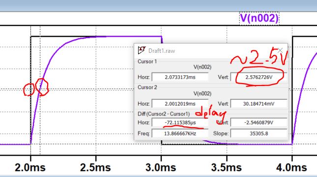
Keep in mind that the delay is measured as the 'time' differences between the input and output at the
50% of the input and the output voltage.
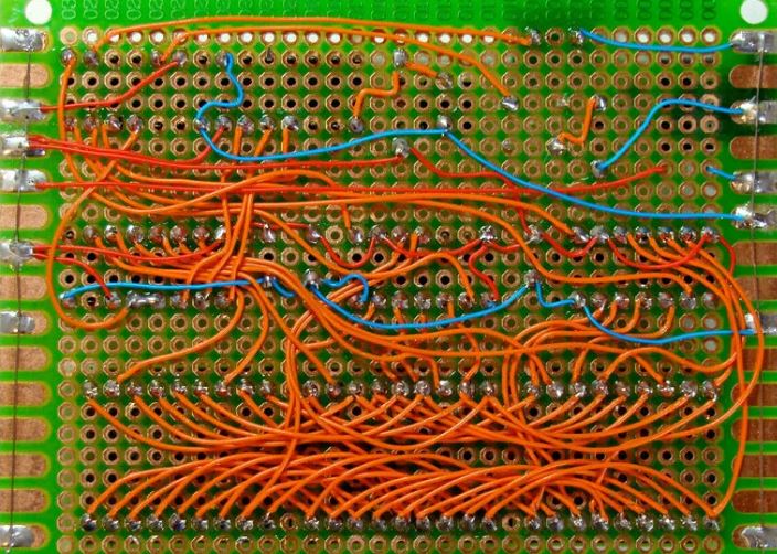
An example of soldering on a prototype PCB and its 'Jumping Wires':
3. Build the following circuit in LTSpice: (just a different input of
the previous task)
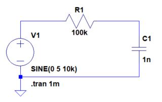
Why the output is attenuated? Can you explain this qualitatively?
What if you decrease the frequency? Does the output increase or
decrease? Why? Explain this qualitatively.
What
if you increase the frequency? Does the output increase or decrease?
Why? Explain this qualitatively.
Build
the circuit on the prototype PCB board and change the frequency of the
input to show at WHICH frequency the output signal starts being
attenuated.
Show your input
and output of this circuit on an oscilloscope.
4.
Build the following circuit in LTSpice:
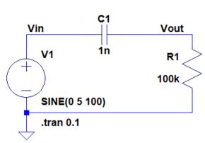
Explain qualitatively why the output is attenuated?
What if you decrease the frequency? Does the output increase or
decrease? Why? Explain this qualitatively.
What
if you increase the frequency? Does the output increase or decrease?
Why? Explain this qualitatively.
Build the circuit on the
prototype PCB board and change the frequency of the input to show at
WHICH frequency the output signal starts being attenuated.
Show your input
and output of this circuit on an oscilloscope.
-- The end of the lab